1/7
GS-R12P
June 2004
This is preliminary information on a new product now in development. Details are subject to change without notice.
FEATURE
MTBF 1 000 000 hours (T
amb
=25
)
C)
1.5A max output current
16V max input voltage
1.5V max drop-out voltage
Remote logic inhibit/enable
Not-latching overload and short circuit
protection
Thermal shutdown
Fixed or adjustable output
No heatsink required
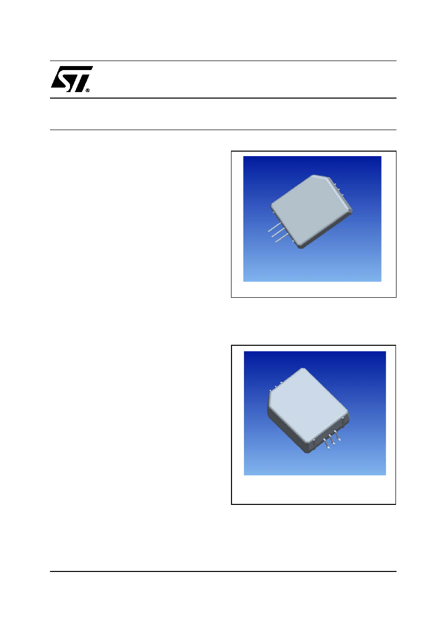
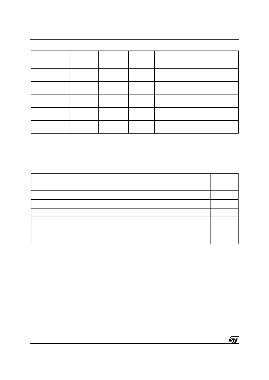
DESCRIPTION
The GS-R12P series is a family of high efficiency
step down switching voltage regulator, designed to
replace linear regulators.
Based on STM L5973 device, this non isolated family
of regulators are suitable for the full spectrum of ap-
plications including telecom, industry, computer and
distributed power system applications having a wide-
ly ranging input voltage.
Packing type: H = horizontal PTH
-------------------
S = horizontal SMD
Packing type: V = vertical PTH
PRELIMINARY
1.8W TO 8W STEP-DOWN SWITCHING REGULATOR FAMILY
GS-R12P
2/7
SELECTION CHART
* Packing Legend (P)
H = horizontal through hole
S = horizontal SMD
V = vertical through hole
ABSOLUTE MAXIMUM RATINGS
Type
Ordering
Number
Output
Voltage
[V]
Input
Voltage
[V]
Output
Ripple
[mVpp]
Efficiency
[%]
Package
(P)*
Notes
GS-R12(P)0181.5
1.8
± 4%
4.5
˜
15
35
72
H-S-V
Fixed output
voltage
GS-R12(P)0251.5
2.5
±
4
%
4.5
˜
15
35
76
H-S-V
Fixed output
voltage
GS-R12(P)0331.5
3.3
±
4
%
4.5
˜
15
35
82
H-S-V
Fixed output
voltage
GS-R12(P)0501.5
5.0
±
4
%
6.6
˜
15
35
85
H-S-V
Fixed output
voltage
GS-R12(P)0001.5
1.235
˜
5.5
4.5
˜
15
35
68
˜
85
H-S
Progr. output
voltage
Symbol
Parameter
Value
Unit
V
i
DC Input Voltage (for GS-R12(P)XXX1.5)
16
V
I
out
Maximum Output Current
int. limit
V
4
INH
-0.3 to V
i
V
V
6
FB
4
V
T
stg
Storage Temperature Range
-40
˜
105
∞C
T
op
Operating Ambient Temperature
-25
˜
70
∞C
T
op1
Operating Ambient Temperature with current derating
-25
˜
85
∞C
3/7
GS-R12P
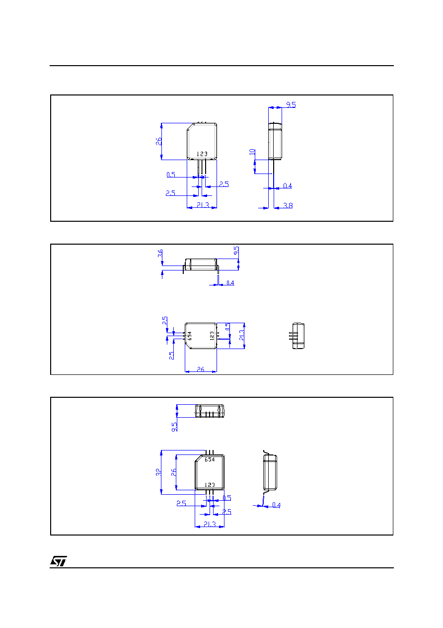
CONNECTION DIAGRAM AND MECHANICAL DATA
GS-R12VXXX1.5
GS-R12HXXX1.5
GS-R12SXXX1.5
GS-R12P
4/7
PIN DESCRIPTION
ELECTRICAL CHARACTERISTICS All versions (T
amb
=25
)
C, unless otherwise specified.)
ELECTRICAL CHARACTERISTICS for horizontal versions only (T
amb
=25
)
C, unless otherwise specified.)
Pin
Function
Description
1
Input +
DC input voltage
2
Input/Output GND
Return for input/output voltage source
3
V
out
Regulated power output
4
INH
A logical level (active high) disables the device, when it is open an internal pull
up disables the device
5
V
out-c
Regulated output point for additional compensation
6
FB
Feedback input, available on adjustable device and on request for additional
compensation
Symbol
Parameter
Test Condition
Min.
Typ.
Max.
Unit
V
r
Ripple Voltage
V
i
=12V I
o
= 1.5A
35
mVpp
Temperature Stability
V
i
=V
o
+ 1.5V I
o
= 1.5A
mV/∞C
I
o
Output Current
V
i
=4.5
˜
16V
0
1.5
A
I
oL
Current Limit
V
i
=4.5
˜
16V
2.5
A
I
q
Quiescent Current
V
i
=12V I
o
= 0A
1.8
2.5
mA
f
s
Switching Frequency
V
i
=12V I
o
= 1.5A
225
250
275
kHz
SRV
Supply Voltage Rejection
mV/V
R
th
Thermal Resistance
Case to ambient
∞C/W
Symbol
Parameter
Test Condition
Min.
Typ.
Max.
Unit
I
qst-by
Total Stand-by Quiescent
Current
V
inh
>2.2V V
i
= 15V
50
100
µ
A
INH
INH Threshold Voltage
Device ON
0.8
V
Device OFF
2.2
V
V
FB
Feedback Voltage
V
i
=4.5
˜
15V I
o
= 0
˜
1.5A
1.22
1.235
1.25
V

5/7
GS-R12P
USER NOTES
Input Voltage
The recommended operating maximum DC Input Voltage is 15V inclusive of ripple voltage.
Inhibit function
The inhibit feature allows to put in stand-by mode the device.
With INH pin 4 higher than 2.2V the device is disabled and the power consumption is reduced to less than
100µA for V
i
= 15V.
With INH pin lower than 0.8V, the device is enabled.
If the INH pin is left floating, an internal pull up ensures that the voltage at the pin reaches the inhibit threshold
and the device is disabled.
The pin is also V
i
compatible.
Current protection
The device has two current limit protections, pulse by pulse and frequency fold back.
The current is sensed through a resistor and if reaches the threshold, the on time is reduced and consequently
the output voltage too.
Since the minimum switch ON time (necessary to avoid false overcurrent signal) is not enough to obtain a suf-
ficiently low duty cycle at 250 Hz, the output current, in strong overcurrent or short circuit conditions, could in-
crease again.
For this reason the switching frequency is also reduced, so keeping the inductor current under its maximum
threshold.
The frequency depends on the feedback voltage.
As the feedback voltage decreases (due to the reduced duty cycle), the switching frequency decrease too.
Thermal shutdown
The shutdown block generates a signal that turns off the power stage if the temperature of the internal chip goes
higher than a fixed internal threshold (150 ∫C).
The sensing element of the chip is very close to the PDMOS area, so ensuring an accurate and fast temperature
detection.
An hysteresis of approximately 20∫C avoids that the devices turns on and off continuously.
Thermal Characteristics
Output voltage programming (GS-R12H(S)0001.5 only)
The GS-R12P output voltage is 5.54V ±4%, to reduce this value connect a resistor between pin 6 (FB) and
pin 5 (V
out-c
).
The resistor must be located very close to the proper pins, to minimize the injected noise (see figure 1).
The resistor value is calculated using the following formula:
Rv=[(V
out
-1.235)*11.3]/(5.54-V
out
)
--
[kOhm]
V
out
can be adjusted between 1.235V (Rv=0 Ohm) and 5.54V (Rv=open)

GS-R12P
6/7
Loop compensation (GS-R12H(S)0001.5 only)
If required by particular load conditions, it is possible to change the feedback loop compensation, adding an ex-
ternal capacitor between pin 6 (FB) and pin 5 (V
out-c
), which will act as speed up (see figure 2).
ADDITIONAL FEATURES AND PROTECTIONS
Feedback disconnection
In case of feedback disconnection, the duty cycle increases versus the maximum allowed value, bringing the
output voltage close to the input supply.
THis condition could destroy the load.
To avoid this dangerous condition, the device is turned off if the internal feedback pin remains floating.
Output overvoltage protection
The overvoltage protection, OVP, is realized by using an internal comparator, which input is connected to the
feedback, that turns off the power stage when the OVP threshold is reached.
This threshold is typically 30% higher than the feedback voltage.
Figure 1
Figure 2

Information furnished is believed to be accurate and reliable. However, STMicroelectronics assumes no responsibility for the con-
sequences of use of such information nor for any infringement of patents or other rights of third parties which may result from its
use. No license is granted by implication or otherwise under any patent or patent rights of STMicroelectronics. Specifications men-
tioned in this publication are subject to change without notice. This publication supersedes and replaces all information previously
supplied. STMicroelectronics products are not authorized for use as critical components in life support devices or systems without
express written approval of STMicroelectronics.
The ST logo is a registered trademark of STMicroelectronics.
All other names are the property of their respective owners
© 2004 STMicroelectronics - All Rights Reserved
STMicroelectronics GROUP OF COMPANIES
Australia - Belgium - Brazil - Canada - China -Czech Republic - Finland - France - Germany - Hong Kong - India - Israel - Italy - Japan
- Malaysia - Malta - Morocco - Singapore - Spain - Sweden - Switzerland - United Kingdom - U.S.A.
http://www.st.com
7/7
GS-R12P