31 W TRIPLE OUTPUT STEP-DOWN SWITCHING REGULATORS
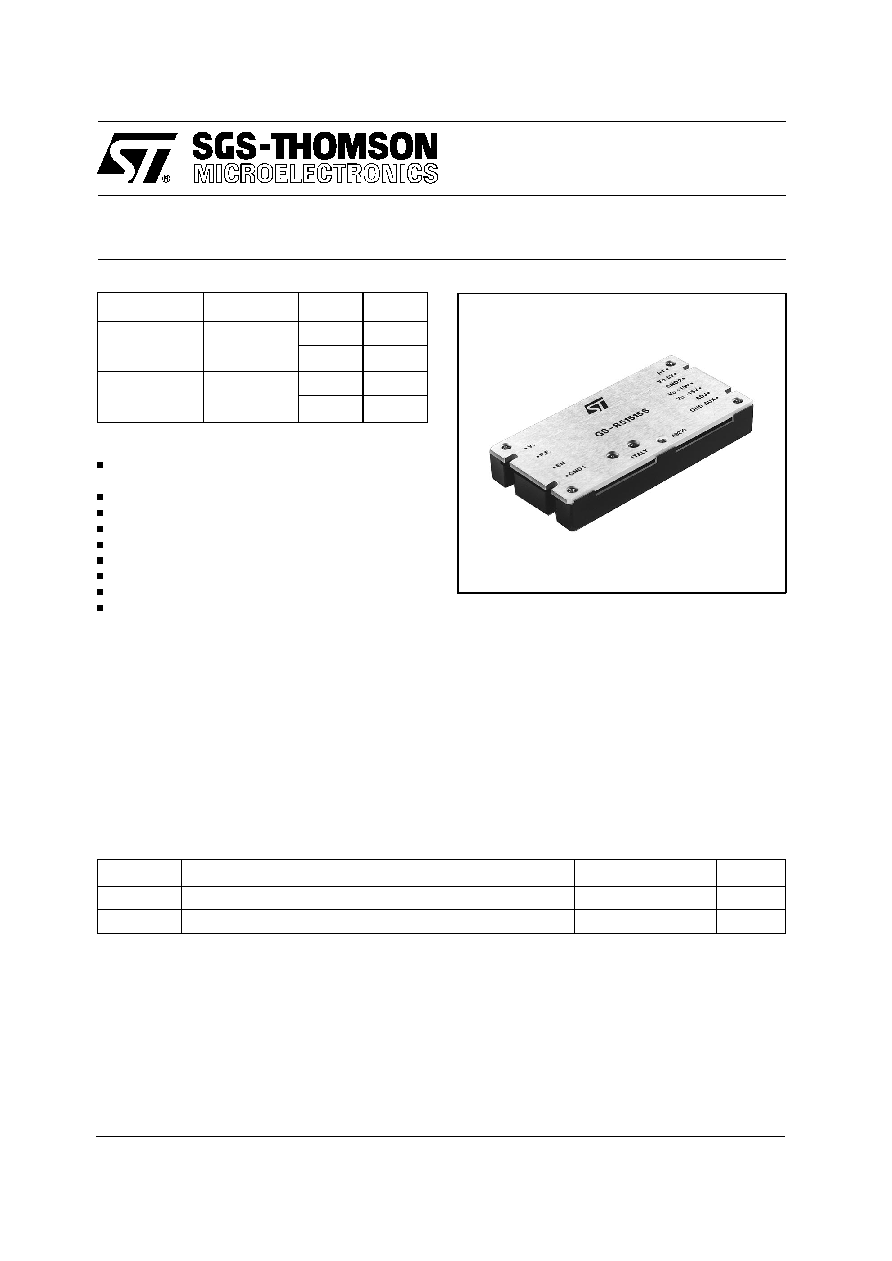
GS-R51212S
GS-R51515S
31W TRIPLE OUTPUT STEP-DOWN SWITCHING REGULATORS
June 1994
1/8
Type
V
i
V
o
I
o
GS-R51212S
15 to 40 V
+ 5,1 V
4,5 A
±
12 V
0,35 A
GS-R51515S
15 to 40 V
+ 5,1 V
4,5 A
±
15 V
0,3 A
FEATURES
5.1V/4.5A and
±
12V/0.35A or
±
15V/0.3A output
voltages
±
12 or
±
15V externally adjustable
High efficiency (81% typ.)
Short-circuit protection
Reset output
Power Fail programmable input
Inhibit/Enable control input
Soft-start
PCB or chassis mounting
DESCRIPTION
The GS-R51212S and GS-R51515S are versatile
triple output, high current step-down switching
regulators that provide +5.1V/4.5A output voltage
and an isolated
±
12V/0.35A or
±
15V/0.3A dual
output voltage.
They are ideal for microprocessor based boards
because power the logic and the communication
ports and have Reset output and Power Fail pro-
grammable input for the correct system start-up.
The Inhibit/Enable pin allows the ON/OFF logic
function with TTL/CMOS compatible input signal.
The auxiliary outputs (
±
12V or
±
15V) are externally
adjustable in a very wide range, i.e. from
±
4.25V to
±
12.45V on GS-R51212S and from
±
4.50V to
±
15.25V (typical values) on GS-R51515S.
ABSOLUTE MAXIMUM RATINGS
Symbol
Parameter
Value
Unit
Vi
DC Input Voltage
44
V
Irs
Reset Output Sink Current
20
mA
2/8
ELECTRICAL CHARACTERISTICS (T
amb
= 25
°
C unless otherwise specified)
Symbol
Parameter
Test Conditions
Min
Typ
Max
Unit
Vi
Input Voltage
GS-R51212S
Vo1 = +5.1V
Io1 = 4.5A
Vo2 = +12V
Io2 = 0.35A
Vo3 = 12V
Io3 = 0.35A
15
40
V
Vi
Input Voltage
GS-R51515S
Vo1 = +5.1V
Io1 = 4.5A
Vo2 = +15V
Io2 = 0.3A
Vo3 = 15V
Io3 = 0.3A
15
40
V
lir
Input Reflected Current
Vi = 24V Io1,2,3 = Full Load
No external input capacitor
0.5
App
lir
Input Reflected Current
Vi = 24V Io1,2,3 = Full Load
Ci (external) = 100
µ
F/50V
0.15
App
Vien
Enable Input Voltage
Vi = 15 to 40V
0
0.8
V
lien
Enable Input Current
Vi = 15 to 40V
1
mA
Viinh
Inhibit Input Voltage
Vi = 15 to 40V
1.2
+Vi
V
Vo1
Output Voltage 1
Vi = 15 to 40V
Io1 = 0 to 4.5A
Io2 = 0 to 0.35/0.3A
Io3 = 0 to 0.35/ 0.3A
+5
+5.1
+5.2
V
Vo2
Output Voltage 2
GS-R51212S
Vi = 15 to 40V
Io1 = 0 to 4.5A
Io2 = 0 to 0.35A Io3 = 0 to 0.35A
+11.5
+12
+12.5
V
Vo2
Output Voltage 2
GS-R51515S
Vi = 15 to 40V
Io1 = 0 to 4.5A
Io2 = 0 to 0.3A
Io3 = 0 to 0.3A
+14.5
+15
+15.5
V
Vo3
Output Voltage 3
GS-R51212S
Vi = 15 to 40V
Io1 = 0 to 4.5A
Io2 = 0 to 0.35A Io3 = 0 to 0.35A
11.5
12
12.5
V
Vo3
Output Voltage 3
GS-R51515S
Vi = 15 to 40V
Io1 = 0 to 4.5A
Io2 = 0 to 0.3A
Io3 = 0 to 0.3A
14.5
15
15.5
V
Vor1
Output Ripple
Voltage 1
Vi = 24V
Io1 = 4.5A
30
50
mVpp
Vor2,3
Output Ripple
Voltage 2,3
Vi = 24V
Io2,3 = 0.35/0.3A
50
100
mVpp
V
OL1
Line Regulation 1
Vi = 15 to 40V
Io1 = 2.5A
Io2,3 = 0.35/0.3A
0.5
mV/V
V
OL2,3
Line Regulation 2,3
Vi = 15 to 40V
Io1 = 2.5A
Io2,3 = 0.35/0.3A
1
mV/V
V
OO1
Load Regulation 1
Vi = 24V
Io1 = 0.5 to 4.5A
Io2,3 = 0.35/0.3A
2
mV/A
V
OO2,3
Load Regulation 2,3
Vi = 24V
Io1 = 2.5A
Io2,Io3 = 0.05 to 0.35/0.3A
500
mV/A
Io1
Output Current 1
Vi = 15 to 40V
Vo1 = 5.1V
Io2,3 = 0 to 0.35/0.3A
0
4.5
A
Io2
Output Current 2*
GS-R51212S
Vi = 15 to 40V
Io1 = 0 to 4.5A
Vo2 = +12V
Io3 = 0 to 0.35A
0
0.35
A
Io2
Output Current 2*
GS-R51515S
Vi = 15 to 40V
Io1 = 0 to 4.5A
Vo2 = +15V
Io3 = 0 to 0.3A
0
0.3
A
Io2
Output Current 2*
GS-R51212S
Vi = 15 to 40V
Io1 = 0 to 4.5A
Vo2 = +12V
Io3 = 0A
0
0.7
A
Io2
Output Current 2*
GS-R51515S
Vi = 15 to 40V
Io1 = 0 to 4.5A
Vo2 = +15V
Io3 = 0A
0
0.6
A
Io3
Output Current 3*
GS-R51212S
Vi = 15 to 40V
Io1 = 0 to 4.5A
Vo3 = 12V
Io2 = 0 to 0.35A
0
0.35
A
GS-R51212S/GS-R51515S
Symbol
Parameter
Test Conditions
Min
Typ
Max
Unit
Io3
Output Current 3*
GS-R51515S
Vi = 15 to 40V
Io1 = 0 to 4.5A
Vo3 = 15V
Io2 = 0 to 0.3A
0
0.3
A
Io3
Output Current 3*
GS-R51212S
Vi = 15 to 40V
Io1 = 0 to 4.5A
Vo3 = 12V
Io2 = 0A
0
0.7
A
Io3
Output Current 3*
GS-R51515S
Vi = 15 to 40V
Io1 = 0 to 4.5A
Vo3 = 15V
Io2 = 0A
0
0.6
A
Iosck1
Output Current
Limit 1
Vi = 15 to 40V
Overload
5.5
A
Iosc1
Output Short-circuit
Current 1
Vi = 15 to 40V
3
A
Iosc2,3
Output Short-circuit
Current 2,3
Vi = 15 to 40V
0.8
A
tss
Soft-start time
10
ms
tdr
Reset Time Delay
100
ms
fs
Switching Frequency
Vi = 15 to 40V
Vo1 = 5.1V
Io1 = 0.5 to 4.5A
Vo2 = +12/+15V Vo3 = 12/ 15V
Io2, Io3 = 0.05 to 0.35/ 0.3A
100
kHz
Efficiency
Vi = 24V
Io1,2,3 = Full Load
78
81
%
Rth
Thermal Resistance
7.5
°
C/W
Tcop
Operating Case
Temperature Range
0
+85
°
C
Tstg
Storage
Temperature Range
40
+105
°
C
* Note: when output current is less than 50mA, output ripple voltage increases due to discontinuous operation.
ELECTRICAL CHARACTERISTICS (T
amb
= 25
°
C unless otherwise specified) (cont'd)
3/8
GS-R51212S/GS-R51515S
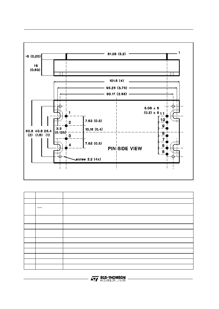
Package R. Dimensions in mm (inches).
CONNECTION DIAGRAM AND MECHANICAL DATA
4/8
PIN DESCRIPTION
Pin
Function
Description
1
GND IN
Return for input voltage source. Internally connected to pin 7.
2
EN.
Inhibit/Enable control input. The converter is ON (ENABLE) when the voltage applied to
this pin is lower than 0.8V. The converter is OFF (INHIBIT) when this pin is unconnected or
the input voltage is in the range of 1.2 to Vi.
3
P.F.
Power Fail programmable input. If unconnected the Power Fail threshold voltage is 11V
with 1V hysteresis (factory setting).
4
+ Vin
DC input voltage. Recommended maximum voltage is 40V.
5
RT
Reset output (active high). When the supply voltage +Vin and the regulated output voltage
+Vo1 are in the correct range this signal is generated after a delay time of 100ms typical.
6
Vo + 5V
Regulated +5.1V output voltage.
7
GND 1
Return for output 1 current path. Internally connected to pin 1.
8
Vo + 12/15V
Regulated +12 or +15V output.
9
Vo 12/15V
Regulated 12 or 15V output.
10
ADJ.
External adjustment for output voltages
±
12 and
±
15V.
11
GND Aux.
Return for
±
12 and
±
15V output current path.
GS-R51212S/GS-R51515S
5/8
USER NOTES
Input Voltage
The recommended operating maximum DC input
voltage is 40V inclusive of the ripple voltage. The
use of an external low ESR, high ripple current
capacitor located as close the module as possible
is recommended; suggested value is 100
µ
F/50V.
Soft-start
To avoid heavy inrush current the output voltage
rise time is typically 10ms in any condition of load.
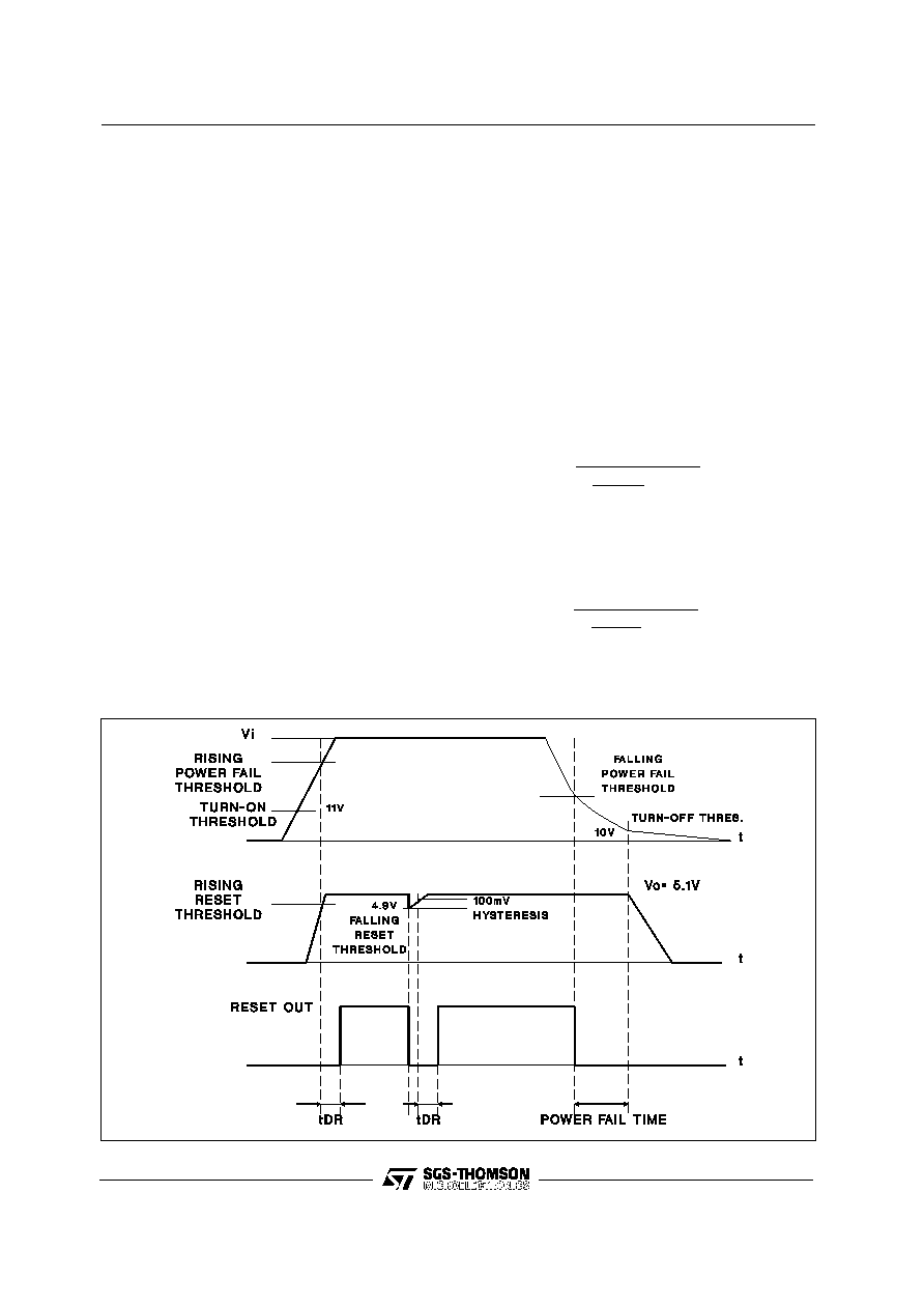
Power Fail-Reset Circuit
The module include a voltage sensing circuit that
may be used to generate a power-on/power-off
reset signal for a microprocessor system.
The circuit sense the input supply voltage and the
output generated voltage Vo1 (+5V) and will gener-
ate the required reset signal only when both the
sensed voltages have reached the required value
for correct system operation.
When both the supply voltage and the regulated
voltage are in the correct range the output Reset
signal is generated after a delay time t
DR
of 100ms
typical.
A latch assures that if a spike is present on the
sensed voltage the delay time circuit discharges
completely before initialization of a new reset cycle.
Reset output has internal pull-up resistor of
10kOhm connected to Vo +5V pin.
Maximum sink output current is 20mA at
V
RESET(sat)
= 200mV.
Fig. 1 and fig. 2 show reset waveforms.
Power Fail Programmable Input
This pin is internally connected via a divider to the
+Vin pin for Power Fail function.
The factory setting is for a value of 11V with 1V
hysteresis.
It is possible to program a different value of Power
Fail threshold by connecting a resistor (Rpf) be-
tween pin 3 (Power Fail Input) and pin 1 (GND
Input). The value of Rpf must be calculated accord-
ing to the following formula:
R
pf
=
5.1
=
(
k
)
V
pf
-
5.1
34
-
0.191
where Vpf is the desired value of Power Fail thresh-
old voltage.
Exampe: Vpf = 24V (must not be lower than 12V):
R
pf
=
5.1
=
14k
24
-
5.1
34
-
0.191
Figure 1 - Reset and Power Fail waveforms.
GS-R51212S/GS-R51515S