HCC/HCF40104B
HCC/HCF40194B
4-BIT BIDIRECTIONAL UNIVERSAL SHIFT REGISTER
DESCRIPTION
.
MEDIUM-SPEED OPERATION : f
CL
= 9MHz
(typ.) @ V
DD
= 10V
.
FULLY STATIC OPERATION
.
SYNCHRONOUS
PARALLEL
OR
SERIAL
OPERATION
.
THREE-STATE OUTPUTS (HCC/HCF40104B)
.
ASYNCHRONOUS
MASTER
RESET
(HCC/HCF40194B)
.
STANDARDIZED, SYMMETRICAL OUTPUT
CHARACTERISTICS
.
QUIESCENT CURRENT AT 20V FOR HCC DE-
VICE
.
5V, 10V, AND 15V PARAMETRIC RATINGS
.
INPUT CURRENT OF 100nA AT 18V AND 25
∞
C
FOR HCC DEVICE
.
100% TESTED FOR QUIESCENT CURRENT
.
MEETS ALL REQUIREMENTS OF JEDEC TEN-
TATIVE STANDARD N
∞
13A, "STANDARD SPE-
CIFICATIONS FOR DESCRIPTION OF "B"
SERIES CMOS DEVICES"
June 1989
The HCC40104B, HCC40194B, (extended tem-
perature range) and the HCC40104B, HCF40194B
(intermediate temperature range) are monolithic in-
tegrated circuits, available in 16-lead dual in-line
plastic or ceramic package and plastic micro pack-
age. The HCC/HCF 40104B is a universal shift reg-
ister featuring parallel inputs, parallel outputs, SHIFT
RIGHT and SHIFT LEFT serial inputs, and a high-im-
pedance third output state allowing the device to be
used in bus-organized systems. In the parallel-load
mode (S0 and S1 are high), data is loaded into the
associated flip-flop and appears at the output after
the positive transition of the CLOCK input. During
loading, serial data flow is inhibited. Shift-right and
shift-left are accomplished synchronously on the
positive clock edge with serial data entered at the
SHIFT RIGHT and SHIFT LEFT serial inputs, re-
spectively. Clearing the register is accomplished by
setting both mode controls low and clocking the reg-
ister. When the output enable input is low, all outputs
assume
the
high
impedance
state.
The
HCC/HCF40194B is a universal shift register featur-
ing parallel inputs, parallel outputs SHIFT RIGHT and
SHIFT LEFT serial inputs, and a direct overriding
clear input. In the parallel-load mode (S0 and S1 are
high), data is loaded into the associated flip-flop and
EY
(Plastic Package)
F
(Ceramic Package)
C1
(Plastic Chip Carrier )
ORDER CODES :
HCC401XXBF
HCF401XXBEY
HCF401XXBC1
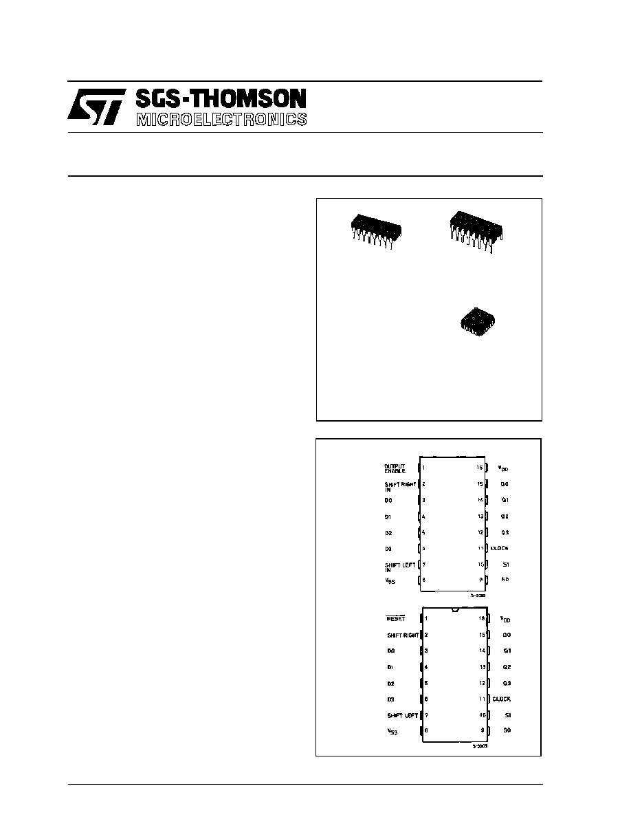
PIN CONNECTIONS
40104B
40194B
1/12
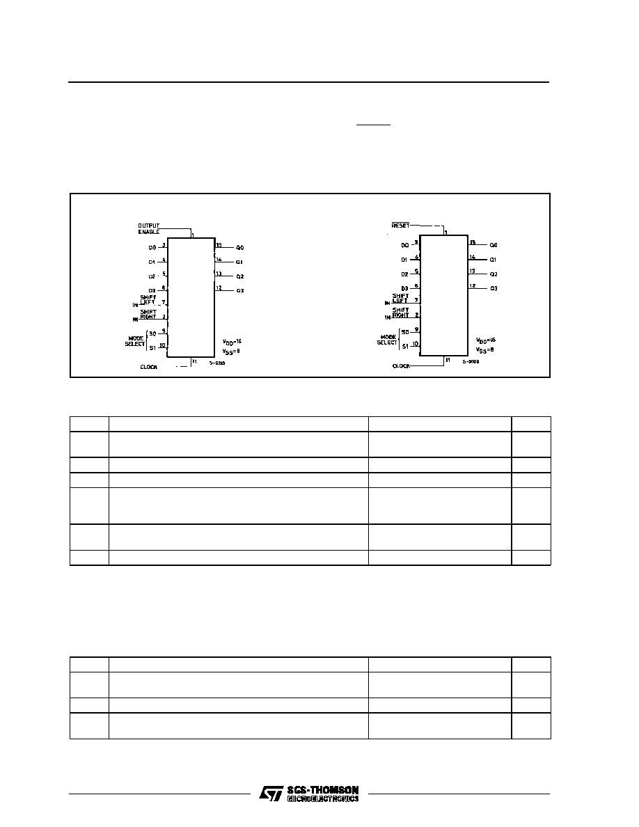
FUNCTIONAL DIAGRAMS
ABSOLUTE MAXIMUM RATINGS
Symbol
Parameter
Val ue
Unit
V
DD
*
Supply Voltage : H CC Types
H C F Types
≠ 0.5 to + 20
≠ 0.5 to + 18
V
V
V
i
Input Voltage
≠ 0.5 to V
DD
+ 0.5
V
I
I
DC Input Current (any one input)
±
10
mA
P
t o t
Total Power Dissipation (per package)
Dissipation per Output Transistor
for T
o p
= Full Package-temperature Range
200
100
mW
mW
T
o p
Operating Temperature : H CC Types
H C F Types
≠ 55 to + 125
≠ 40 to + 85
∞
C
∞
C
T
s t g
Storage Temperature
≠ 65 to + 150
∞
C
40104B
40194B
Stresses above those listed under "Absolute Maximum Ratings" may cause permanent damage to the device. This is a stress
rating only and functional operation of the device at these or any other conditions above those indicated in the operational sec-
tions of this specifi cation is not implied. Exposure to absolute maximum rating conditions for external periods may affect device
reliability.
* All voltages values are referred to V
SS
pin voltage.
appears at the output after the positive transition of
the CLOCK input. During loading, serial data flow is
inhibited. Shift right and shift left are accomplished
synchronously on the positive clock edge with data
entered at the SHIFT RIGHT and SHIFT LEFT serial
inputs, respectively. Clocking of the register is in-
hibited when both mode control inputs are low. When
low, the RESET input resets all stages and forces all
outputs low. The HCC/HCF40194B is similar to in-
dustry types 340194 and MC40194.
RECOMMENDED OPERATING CONDITIONS
Symbol
Parameter
Val ue
Unit
V
DD
Supply Voltage : HC C Types
H C F Types
3 to 18
3 to 15
V
V
V
I
Input Voltage
0 to V
DD
V
T
o p
Operating Temperature : H CC Types
H C F Types
≠ 55 to + 125
≠ 40 to + 85
∞
C
∞
C
HCC/HCF40104B/40194B
2/12
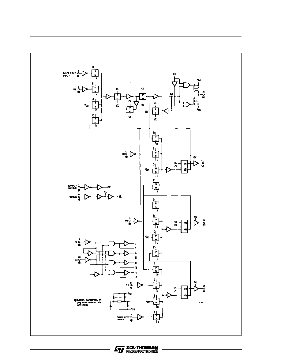
LOGIC DIAGRAMS
40104B
HCC/HCF40104B/40194B
3/12
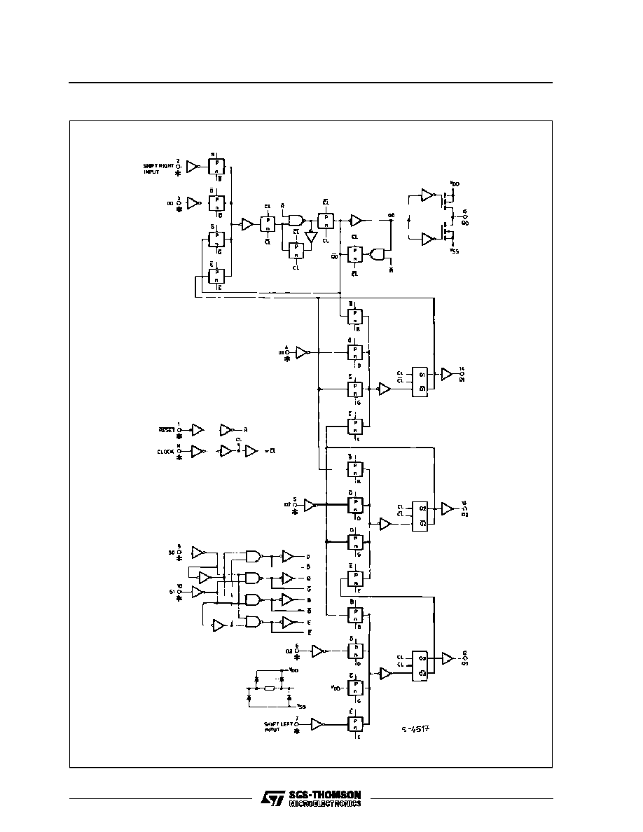
LOGIC DIAGRAMS
40194B
HCC/HCF40104B/40194B
4/12
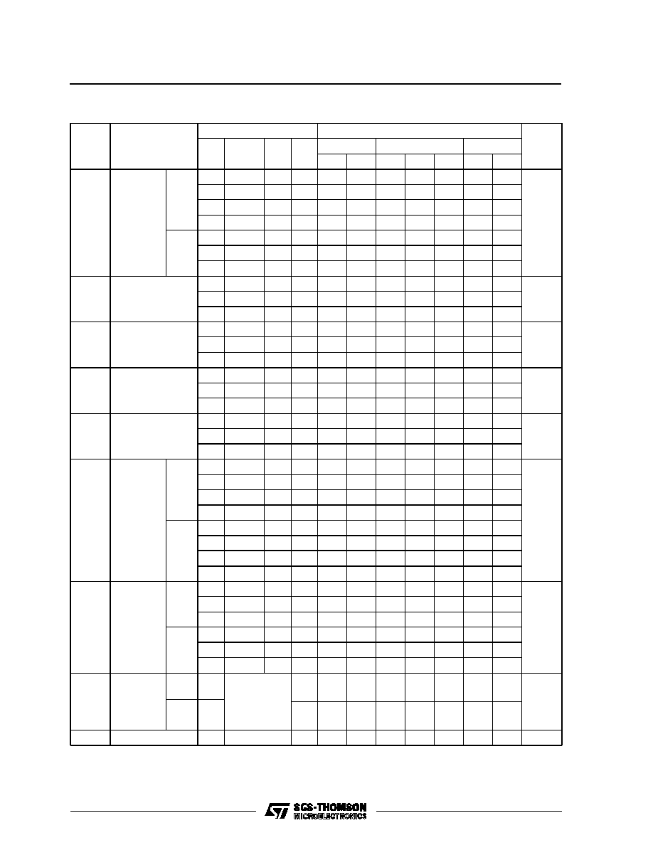
STATIC ELECTRICAL CHARACTERISTICS (over recommended operating conditions)
Test Conditions
Value
V
I
V
O
|I
O
|
V
D D
T
L o w
*
25
∞
C
T
Hi g h
*
Symbol
Parameter
(V)
(V)
(
µ
A)
(V)
Min. Max. Min. Typ. Max. Min. Max.
Unit
I
L
Quiescent
Current
HCC
Types
0/ 5
5
5
0.04
5
150
µ
A
0/10
10
10
0.04
10
300
0/15
15
20
0.04
20
600
0/20
20
100
0.08
100
3000
HCF
Types
0/ 5
5
20
0.04
20
150
0/10
10
40
0.04
40
300
0/15
15
80
0.04
80
600
V
O H
Output High
Voltage
0/ 5
< 1
5
4.95
4.95
4.95
V
0/10
< 1
10
9.95
9.95
9.95
0/15
< 1
15
14.95
14.95
14.95
V
O L
Output Low
Voltage
5/0
< 1
5
0.05
0.05
0.05
V
10/0
< 1
10
0.05
0.05
0.05
15/0
< 1
15
0.05
0.05
0.05
V
IH
Input High
Voltage
0.5/4.5
< 1
5
3.5
3.5
3.5
V
1/9
< 1
10
7
7
7
1.5/13.5
< 1
15
11
11
11
V
IL
Input Low
Voltage
4.5/0.5
< 1
5
1.5
1.5
1.5
V
9/1
< 1
10
3
3
3
13.5/1.5
< 1
15
4
4
4
I
O H
Output
Drive
Current
HCC
Types
0/ 5
2.5
5
≠ 2
≠ 1.6 ≠ 3.2
≠ 1.15
mA
0/ 5
4.6
5
≠ 0.64
≠ 0.51 ≠ 1
≠ 0.36
0/10
9.5
10
≠ 1.6
≠ 1.3 ≠ 2.6
≠ 0.9
0/15
13.5
15
≠ 4.2
≠ 3.4 ≠ 6.8
≠ 2.4
HCF
Types
0/ 5
2.5
5
≠ 1.53
≠ 1.36 ≠ 3.2
≠ 1.1
0/ 5
4.6
5
≠ 0.52
≠ 0.44 ≠ 1
≠ 0.36
0/10
9.5
10
≠ 1.3
≠ 1.1 ≠ 2.6
≠ 0.9
0/15
13.5
15
≠ 3.6
≠ 3.0 ≠ 6.8
≠ 2.4
I
O L
Output
Sink
Current
HCC
Types
0/ 5
0.4
5
0.64
0.51
1
0.36
mA
0/10
0.5
10
1.6
1.3
2.6
0.9
0/15
1.5
15
4.2
3.4
6.8
2.4
HCF
Types
0/ 5
0.4
5
0.52
0.44
1
0.36
0/10
0.5
10
1.3
1.1
2.6
0.9
0/15
1.5
15
3.6
3.0
6.8
2.4
I
IH
, I
IL
Input
Leakage
Current
HCC
Types
0/18
Any Input
18
±
0.1
±
10
≠ 5
±
0.1
±
1
µ
A
HCF
Types
0/15
15
±
0.3
±
10
≠ 5
±
0.3
±
1
C
I
Input Capacitance
Any Input
5
7.5
pF
*
T
LOW
= ≠ 55
∞
C for HCC device : ≠ 40
∞
C for HCF device.
*
T
HIGH
= + 125
∞
C for HCC device : + 85
∞
C for HCF device.
The noise Margin for both "1" and "0" level is : 1V min. with V
DD
= 5V, 2V min. with V
DD
= 10V, 2.5 min. with V
DD
= 15V
HCC/HCF40104B/40194B
5/12

DYNAMIC ELECTRICAL CHARACTERISTICS (T
amb
= 25
∞
C, C
L
= 50pF, R
L
= 200k
,
typical temperature coefficient for all V
DD
values is 0.3%/
∞
C, all input rise and fall time = 20ns)
Test Conditions
Val ue
Symbol
Parameter
V
D D
(V)
Min.
Typ.
Max.
Unit
t
PL H
,t
P HL
Propagation Delay Time
Clock to Q
5
220
440
ns
10
100
200
15
70
140
t
PZ H
, t
PZ L
,
t
PL Z
3-state Outputs
s
High Impedance
5
80
160
ns
10
35
70
15
25
50
t
P HZ
5
45
90
ns
10
25
50
15
20
40
t
T HL
, t
TL H
Transition Time
5
100
200
ns
10
50
100
15
40
80
t
se t u p
Setup Time D0,D3,SR, SL
to Clock
5
80
100
ns
10
35
70
15
20
50
S0, S1 to Clock
5
200
400
ns
10
110
220
15
65
130
t
h o l d
Hold Time D0,D3,SR, SL
to Clock
5
≠ 65
0
ns
10
≠ 25
0
15
≠ 15
0
S0, S1 to Clock
5
≠ 170
0
ns
10
≠ 95
0
15
≠ 55
0
t
W
Clock Pulse Width
5
90
180
ns
10
40
180
15
25
50
f
CL
Clock Input Frequency
5
3
6
MHz
10
6
12
15
8
15
t
r
, t
f
Clock Input Rise or Fall Time
5
1000
µ
s
10
100
15
100
t
W
Reset Pulse Width*
5
150
300
ns
10
100
200
15
70
140
t
PRHL
Propagation Delay Reset*
5
230
460
ns
10
90
180
15
65
130
s
For 40104B series only
* For 40194B series only.
HCC/HCF40104B/40194B
6/12
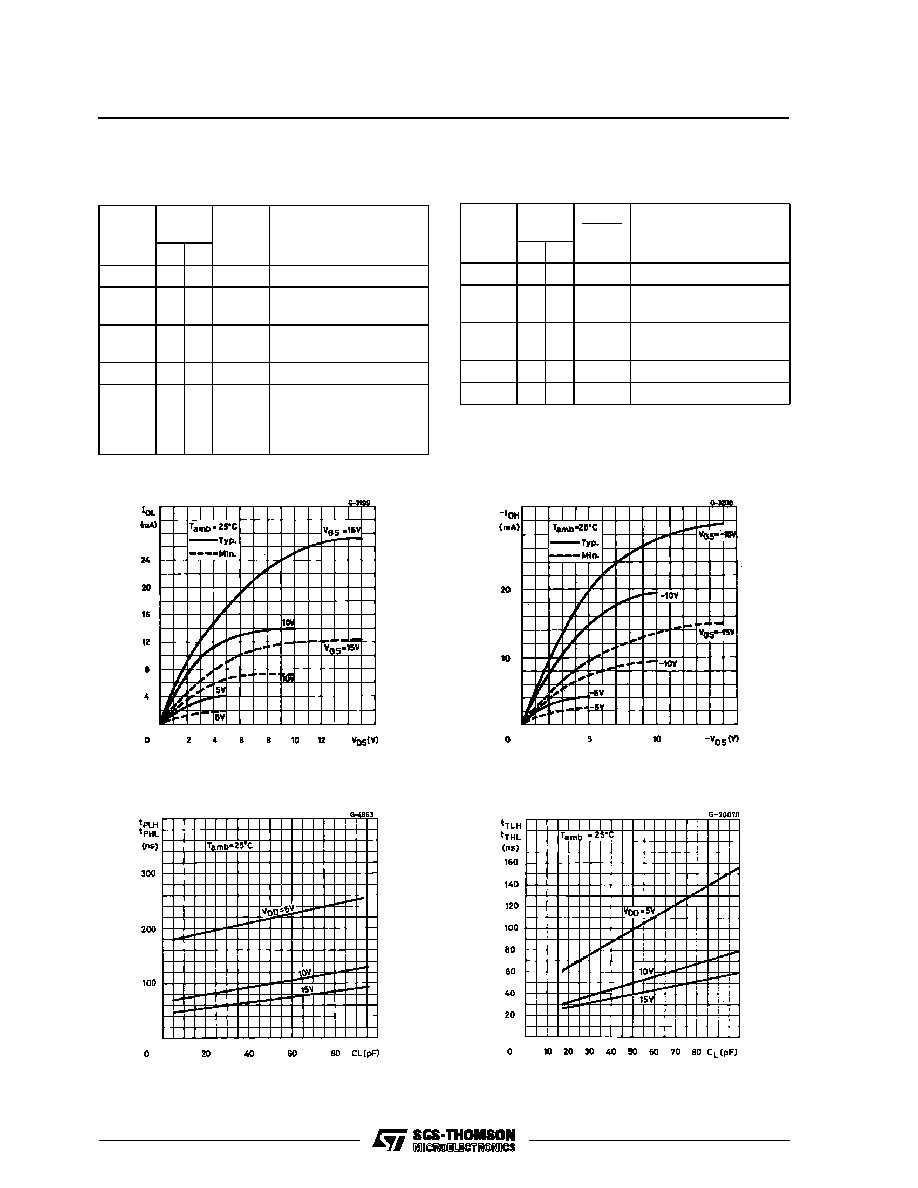
Output Low (sink) Current Characteristics.
Output High (source) Current Characteristics.
Typical Propagation Delay Time vs. Load Capacit-
ance.
Typical Transition Time vs. Load Capacitance.
TRUTH TABLES
40104B
Mode
Select
Clock
v
S 0 S 1
O utput
E nable
Action
≠
/
≠
0
0
1
Reset
≠
/
≠
1
0
1
Shift Right
(Q0 toward Q3)
≠
/
≠
0
1
1
Shift Left
(Q3 toward Q0)
≠
/
≠
1
1
1
Parallel Load
X
X
X
0
Operations occur as
shown above, but
outputs assume high
impedance
40194B
Mode
Select
Clock
S 0 S 1
Reset
Action
X
0
0
1
No Change
≠
/
≠
1
0
1
Shift Right
(Q0 toward Q3)
≠
/
≠
0
1
1
Shift Left
(Q3 toward Q0)
≠
/
≠
1
1
1
Parallel Load
X
X
X
0
Reset
1=High level
X= Don't care
0=Low level
= Level change
HCC/HCF40104B/40194B
7/12
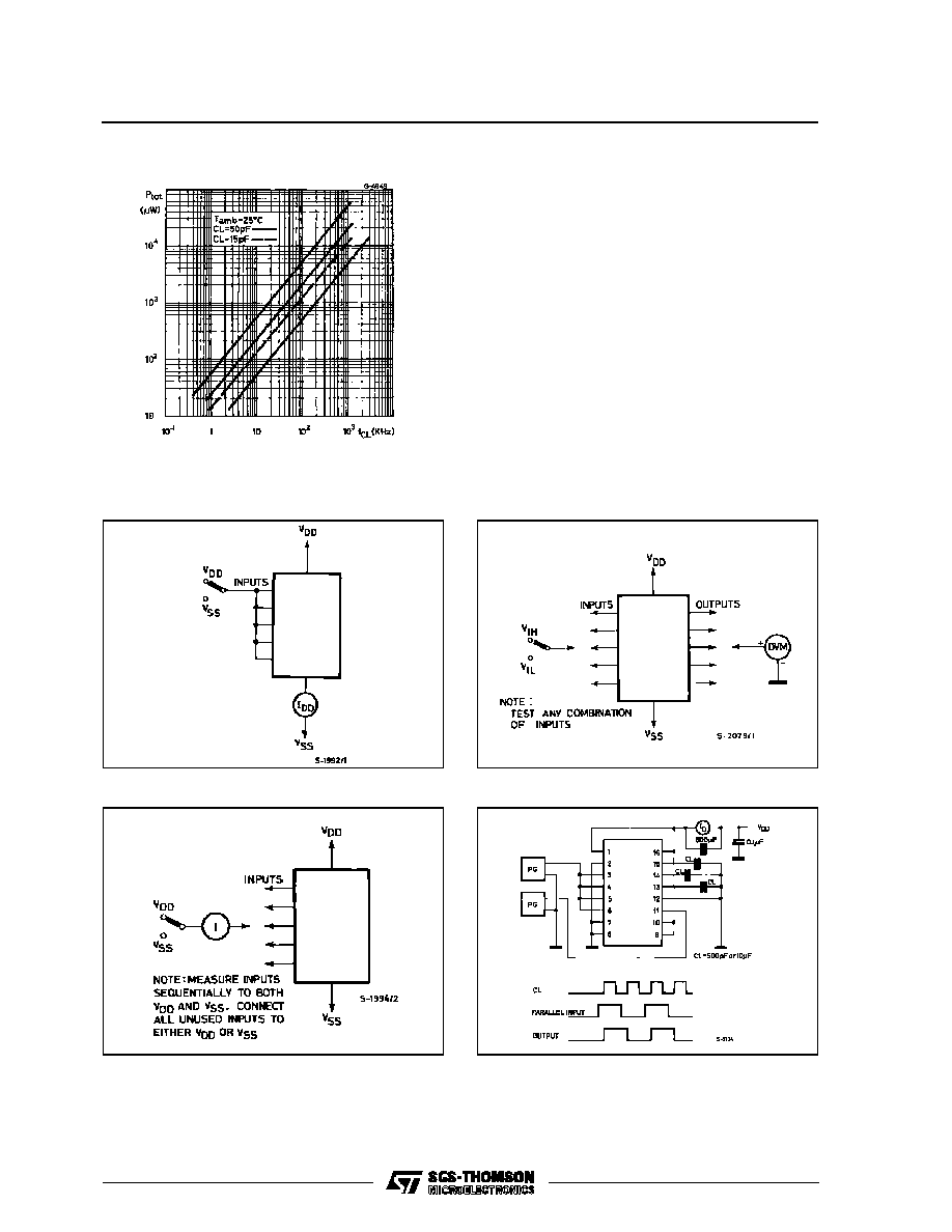
Typical Dynamic Power Dissipation vs. Frequency.
TEST CIRCUITS
Quiescent Device Current.
Input Leakage Current.
Input Voltage.
Dynamic Power Dissipation.
HCC/HCF40104B/40194B
8/12
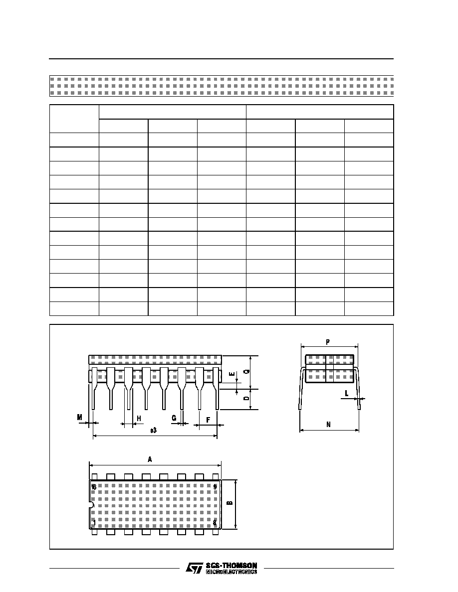
Plastic DIP16 (0.25) MECHANICAL DATA
DIM.
mm
inch
MIN.
TYP.
MAX.
MIN.
TYP.
MAX.
a1
0.51
0.020
B
0.77
1.65
0.030
0.065
b
0.5
0.020
b1
0.25
0.010
D
20
0.787
E
8.5
0.335
e
2.54
0.100
e3
17.78
0.700
F
7.1
0.280
I
5.1
0.201
L
3.3
0.130
Z
1.27
0.050
P001C
HCC/HCF40104B/40194B
9/12
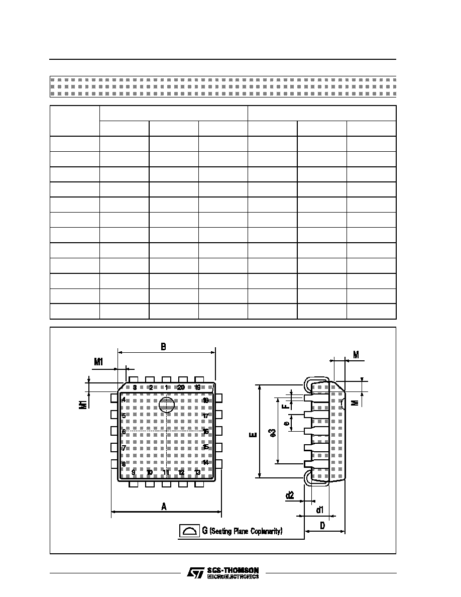
Ceramic DIP16/1 MECHANICAL DATA
DIM.
mm
inch
MIN.
TYP.
MAX.
MIN.
TYP.
MAX.
A
20
0.787
B
7
0.276
D
3.3
0.130
E
0.38
0.015
e3
17.78
0.700
F
2.29
2.79
0.090
0.110
G
0.4
0.55
0.016
0.022
H
1.17
1.52
0.046
0.060
L
0.22
0.31
0.009
0.012
M
0.51
1.27
0.020
0.050
N
10.3
0.406
P
7.8
8.05
0.307
0.317
Q
5.08
0.200
P053D
HCC/HCF40104B/40194B
10/12
PLCC20 MECHANICAL DATA
DIM.
mm
inch
MIN.
TYP.
MAX.
MIN.
TYP.
MAX.
A
9.78
10.03
0.385
0.395
B
8.89
9.04
0.350
0.356
D
4.2
4.57
0.165
0.180
d1
2.54
0.100
d2
0.56
0.022
E
7.37
8.38
0.290
0.330
e
1.27
0.050
e3
5.08
0.200
F
0.38
0.015
G
0.101
0.004
M
1.27
0.050
M1
1.14
0.045
P027A
HCC/HCF40104B/40194B
11/12

Information furnished is believed to be accurate and reliable. However, SGS-THOMSON Microelectronics assumes no responsability for the
consequences of use of such information nor for any infringement of patents or other rights of third parties which may results from its use. No
license is granted by implication or otherwise under any patent or patent rights of SGS-THOMSON Microelectronics. Specifications mentioned
in this publication are subject to change without notice. This publication supersedes and replaces all information previously supplied.
SGS-THOMSON Microelectronics products are not authorized for use as critical components in life support devices or systems without express
written approval of SGS-THOMSON Microelectonics.
©
1994 SGS-THOMSON Microelectronics - All Rights Reserved
SGS-THOMSON Microelectronics GROUP OF COMPANIES
Australia - Brazil - France - Germany - Hong Kong - Italy - Japan - Korea - Malaysia - Malta - Morocco - The Netherlands -
Singapore - Spain - Sweden - Switzerland - Taiwan - Thailand - United Kingdom - U.S.A
HCC/HCF40104B/40194B
12/12