HCC4011B/12B/23B
HCF4011B/12B/23B
NAND GATES
DESCRIPTION
.
PROPAGATION DELAY TIME = 60ns (typ.) AT
C
L
= 50pF, V
DD
= 10V
.
BUFFERED INPUTS AND OUTPUTS
.
QUIESCENT CURRENT SPECIFIED TO 20V
FOR HCC DEVICE
.
INPUT CURRENT OF 100nA AT 18V AND 25
∞
C
FOR HCC DEVICE
.
100% TESTED FOR QUIESCENT CURRENT
.
5V, 10V AND 15V PARAMETRIC RATINGS
.
MEETS ALL REQUIREMENTS OF JEDEC TEN-
TATIVE STANDARD N
o
. 13A, "STANDARD
SPECIFICATIONS FOR DESCRIPTION OF "B"
SERIES CMOS DEVICES"
QUAD 2 INPUT HCC/HCF 4011B
DUAL 4 INPUT HCC/HCF 4012B
TRIPLE 3 INPUT HCC/HCF 4023B
June 1989
The HCC4011B, HCC4012B and HCC4023B (ex-
tended
temperature
range)
and
HCF4011B,
HCF4012B and HCF4023B (intermediate tempera-
ture range) are monolithic, integrated circuit, avail-
able in 14-lead dual in-line plastic or ceramic
package and plastic micropackage.
The
HCC/HCF4011B,
HCC/HCF4012B
and
HCC/HCF4023B NAND gates provide the system
designer with direct implementation of the NAND
function and supplement the existing family of
COS/MOS gates. All inputs and outputs are buf-
fered.
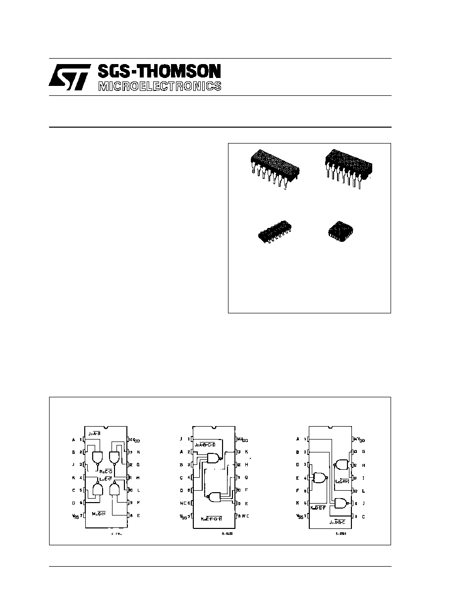
PIN CONNECTIONS
EY
(Plastic Package)
F
(Ceramic Frit Seal Package)
M1
(Micro Package)
C1
(Plastic Chip Carrier)
ORDER CODES :
HCC40XXBF
HCF40XXBM1
HCF40XXBEY
HCF40XXBC1
4011B
4012B
4023B
1/12
ABSOLUTE MAXIMUM RATINGS
Symbol
Parameter
Value
Unit
V
DD
*
Supply Voltage : HC C Types
H CF Types
≠ 0.5 to + 20
≠ 0.5 to + 18
V
V
V
i
Input Voltage
≠ 0.5 to V
DD
+ 0.5
V
I
I
DC Input Current (any one input)
±
10
mA
P
t o t
Total Power Dissipation (per package)
Dissipation per Output Transistor
for T
o p
= Full Package-temperature Range
200
100
mW
mW
T
o p
Operating Temperature : HCC Types
H CF Types
≠ 55 to + 125
≠ 40 to + 85
∞
C
∞
C
T
s t g
Storage Temperature
≠ 65 to + 150
∞
C
RECOMMENDED OPERATING CONDITIONS
Symbol
Parameter
Val ue
Unit
V
DD
Supply Voltage : HC C Types
H C F Types
3 to 18
3 to 15
V
V
V
I
Input Voltage
0 to V
DD
V
T
o p
Operating Temperature : HC C Types
H C F Types
≠ 55 to + 125
≠ 40 to + 85
∞
C
∞
C
Stresses above those listed under "Absolute Maximum Ratings" may cause permanent damage to the device. This is a stress rating only and
functional operation of the device at these or any other conditions above those indicated in the operational sections of this specification is not implied.
Exposure to absolute maximum rating conditions for external periods may affect device reliability.
* All voltage values are referred to V
SS
pin voltage.
HCC/HFC4011B/12B/23B
2/12

STATIC ELECTRICAL CHARACTERISTICS (over recommended operating conditions)
Test Conditions
Value
V
I
V
O
|I
O
|
V
D D
T
L o w
*
25
∞
C
T
Hi g h
*
Symbol
Parameter
(V)
(V)
(
µ
A)
(V)
Min. Max. Min. Typ. Max. Min. Max.
Unit
I
L
Quiescent
Current
HCC
Types
0/5
5
0.25
0.01
0.25
7.5
µ
A
0/10
10
0.5
0.01
0.5
15
0/15
15
1
0.01
1
30
0/20
20
5
0.02
5
150
HCF
Types
0/ 5
5
1
0.01
1
7.5
0/10
10
2
0.01
2
15
0/15
15
4
0.01
4
30
V
O H
Output High
Voltage
0/5
< 1
5
4.95
4.95
4.95
V
0/10
< 1
10
9.95
9.95
9.95
0/15
< 1
15
14.95
14.95
14.95
V
O L
Output Low
Voltage
5/0
< 1
5
0.05
0.05
0.05
V
10/0
< 1
10
0.05
0.05
0.05
15/0
< 1
15
0.05
0.05
0.05
V
IH
Input High
Voltage
0.5/4.5
< 1
5
3.5
3.5
3.5
V
1/9
< 1
10
7
7
7
1.5/13.5
< 1
15
11
11
11
V
IL
Input Low
Voltage
4.5/0.5
< 1
5
1.5
1.5
1.5
V
9/1
< 1
10
3
3
3
13.5/1.5
< 1
15
4
4
4
I
O H
Output
Drive
Current
HCC
Types
0/5
2.5
5
≠ 2
≠ 1.6 ≠ 3.2
≠ 1.15
mA
0/5
4.6
5
≠ 0.64
≠ 0.51 ≠ 1
≠ 0.36
0/10
9.5
10
≠ 1.6
≠ 1.3 ≠ 2.6
≠ 0.9
0/15
13.5
15
≠ 4.2
≠ 3.4 ≠ 6.8
≠ 2.4
HCF
Types
0/5
2.5
5
≠ 1.53
≠ 1.36 ≠ 3.2
≠ 1.1
0/5
4.6
5
≠ 0.52
≠ 0.44 ≠ 1
≠ 0.36
0/10
9.5
10
≠ 1.3
≠ 1.1 ≠ 2.6
≠ 0.9
0/15
13.5
15
≠ 3.6
≠ 3.0 ≠ 6.8
≠ 2.4
I
O L
Output
Sink
Current
HCC
Types
0/5
0.4
5
0.64
0.51
1
0.36
mA
0/10
0.5
10
1.6
1.3
2.6
0.9
0/15
1.5
15
4.2
3.4
6.8
2.4
HCF
Types
0/5
0.4
5
0.52
0.44
1
0.36
0/10
0.5
10
1.3
1.1
2.6
0.9
0/15
1.5
15
3.6
3.0
6.8
2.4
I
IH
, I
IL
Input
Leakage
Current
HCC
Types
0/18
Any Input
18
±
0.1
±
10
≠ 5
±
0.1
±
1
µ
A
HCF
Types
0/15
15
±
0.3
±
10
≠ 5
±
0.3
±
1
C
I
Input Capacitance
Any Input
5
7.5
pF
* T
LOW
= ≠ 55
∞
Cfor HCC device : ≠ 40
∞
C for HCF device.
* T
HIGH
= + 125
∞
C for HCC device : + 85
∞
C for HCF device.
The Noise Margin for both "1" and "0" level is : 1V min. with V
DD
= 5V, 2V min. with V
DD
= 10V, 2.5V with V
DD
= 15V.
HCC/HFC4011B/12B/23B
4/12
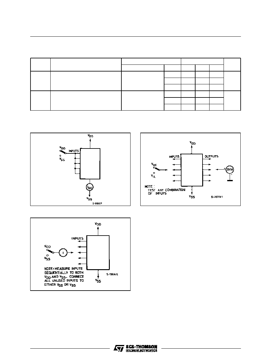
TEST CIRCUITS
Quiescent Device Current.
Noise Immunity.
Input Leakage Current.
DYNAMIC ELECTRICAL CHARACTERISTICS (T
amb
= 25
∞
C, C
L
= 50pF, R
L
= 200k
,
typical temperature coefficient for all V
D D
values is 0.3%/
∞
C, all input rise and fall times = 20ns)
Val ue
Symbol
Parameter
Test Conditions
V
D D
(V)
Min.
Typ.
Max.
Unit
t
PL H
, t
P HL
Propagation Delay Time
5
125
250
ns
10
60
120
15
45
90
t
THL
, t
T L H
Transition Time
5
100
200
ns
10
50
100
15
40
80
HCC/HCF4011B/12B/23B
5/12