 | –≠–ª–µ–∫—Ç—Ä–æ–Ω–Ω—ã–π –∫–æ–º–ø–æ–Ω–µ–Ω—Ç: HCC4031B | –°–∫–∞—á–∞—Ç—å:  PDF PDF  ZIP ZIP |
HCC/HCF4031B
64-STAGE STATIC SHIFT REGISTER
DESCRIPTION
.
FULLY STATIC OPERATION : DC to 16MHz
(TYP.) @ V
DD
≠ V
SS
= 15V
.
STANDARD TTL DRIVE CAPABILITY ON Q
OUTPUT
.
RECIRCULATION CAPABILITY
.
THREE CASCADING MODES :
DIRECT
CLOCKING
FOR
HIGH-SPEED
OPERATION
DELAYED CLOCKING FOR REDUCED CLOCK
DRIVE REQUIREMENTS
ADDITIONAL 1/2 STAGE FOR SLOW CLOCKS
.
QUIESCENT CURRENT SPECIFIED TO 20V
FOR HCC DEVICE
.
STANDARDIZED, SYMMETRICAL OUTPUT
CHARACTERISTICS
.
5V, 10V, AND 15V PARAMETRIC RATINGS
.
INPUT CURRENT OF 100nA at 18V AND 25
∞
C
FOR HCC DEVICE
.
100% TESTED FOR QUIESCENT CURRENT
.
MEETS ALL REQUIREMENTS OF JEDEC TEN-
TATIVE STANDARD N
O
. 13A, "STANDARD
SPECIFICATIONS FOR DESCRIPTION OF "B"
SERIES CMOS DEVICES"
June 1989
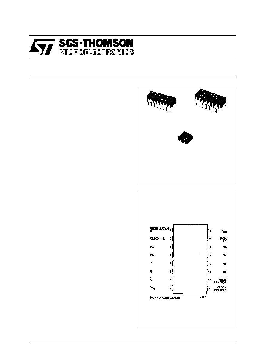
The HCC4031B (extended temperature range) and
HCF4031B (intermediate temperature range) are
monolithic integrated circuits, available in 16-lead
dual in-line plastic or ceramic package.
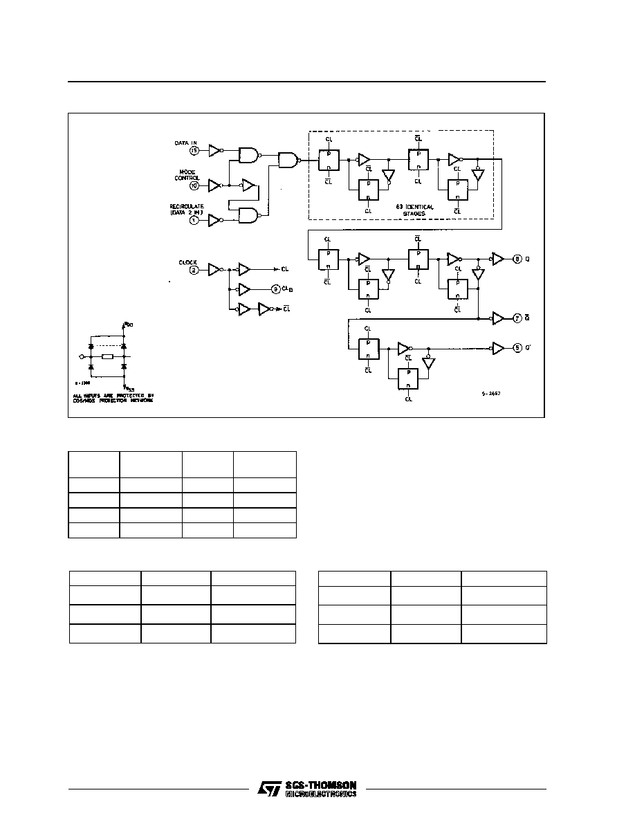
The HCC/HCF4031B is a static shift register that
contains 64 D-type, master-slave flip-flop stages
and one stage which is a D-type master flip-flop only
(referred to as a 1/2 stage). The logic level present
at the DATA input is transferred into the first stage
and shifted one stage at each positive-going clock
transition. Maximum clock frequencies up to 16
Megahertz (typical) can be obtained. Because fully
static operation is allowed, information can be per-
manently stored with the clock line in either the low
or high state. The HCC/HCF4031B has a MODE
CONTROL input that, when in the high state, allows
operation in the recirculating mode. The MODE
CONTROL input can also be used to select between
two separate data sources. Register packages can
be cascaded and the clock lines driven directly for
high-speed operation. Alternatively, a delayed clock
output (CL
D
) is provided that enables cascading reg-
EY
(Plastic Package)
F
(Ceramic Package)
C1
(Chip Carrier)
ORDER CODES :
HCC4031BF
HCF4031BEY
HCF4031BC1
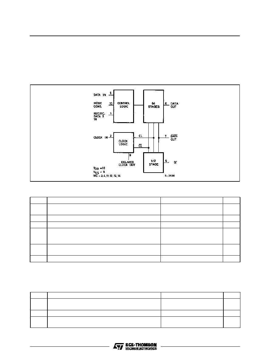
PIN CONNECTIONS
1/12
FUNCTIONAL DIAGRAM
ABSOLUTE MAXIMUM RATINGS
Symbol
Parameter
Value
Unit
V
DD
*
Supply Voltage : HC C Types
H C F Types
≠ 0.5 to + 20
≠ 0.5 to + 18
V
V
V
I
Input Voltage
≠ 0.5 to V
DD
+ 0.5
V
I
I
DC Input Current (any one input)
±
10
mA
P
t o t
Total Power Dissipation (per package)
Dissipation per Output Transistor
for T
o p
= Full Package-temperature Range
200
100
mW
mW
T
o p
Operating Temperature : HCC Types
H CF Types
≠ 55 to + 125
≠ 40 to + 85
∞
C
∞
C
T
s t g
Storage Temperature
≠ 65 to + 150
∞
C
RECOMMENDED OPERATING CONDITIONS
Symbol
Parameter
Val ue
Unit
V
DD
Supply Voltage : HCC Types
HC F Types
3 to + 18
3 to + 15
V
V
V
I
Input Voltage
0 to V
DD
V
T
o p
Operating Temperature : H CC Types
H C F Types
≠ 55 to + 125
≠ 40 to + 85
∞
C
∞
C
Stresses above those listed under "Absolute Maximum Ratings" may cause permanent damage to the device. This is a stress rating only and
functional operation of the device at theseor any other conditions abovethose indicated in the operational sections of this specification is not implied.
Exposure to absolute maximum rating conditions for external periods may affect device reliability.
* All voltage values are referred to V
SS
pin voltage.
ister packages while allowing reduced clock drive
fan-out and transition-time requirements. A third
cascading option makes use of the Q' output from
the 1/2 stage, which is available on the next nega-
tive-going transition of the clock after the Q output
occurs. This delayed output, like the delayed clock
CL
D
, is used with clocks having slow rise and fall
times.
HCC/HCF4031B
2/12
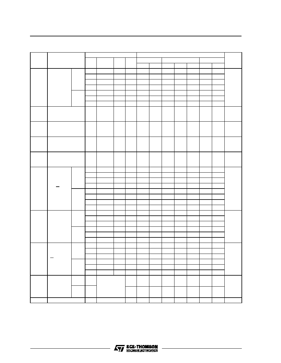
LOGIC DIAGRAM AND TRUTH TABLES
INPUT CONTROL CIRCUIT
Data
Recirc.
Mode
Bit Into
Stage 1
1
X
0
1
0
X
0
0
X
1
1
1
X
0
1
0
TYPICAL STAGE
D a ta
C L
D a ta + 1
0
≠
/
≠
0
1
≠
/
≠
1
X
≠\
≠
NC
OUTPUT FROM Q' (pin 5)
Data + 6 4
CL
Data + 64.5
0
≠\
≠
0
1
≠\
≠
1
X
≠
/
≠
NC
1 = HIGH LEVEL
0 = LOW LEVEL
NC = NO CHANGE
X = DON'T CARE
HCC/HCF4031B
3/12
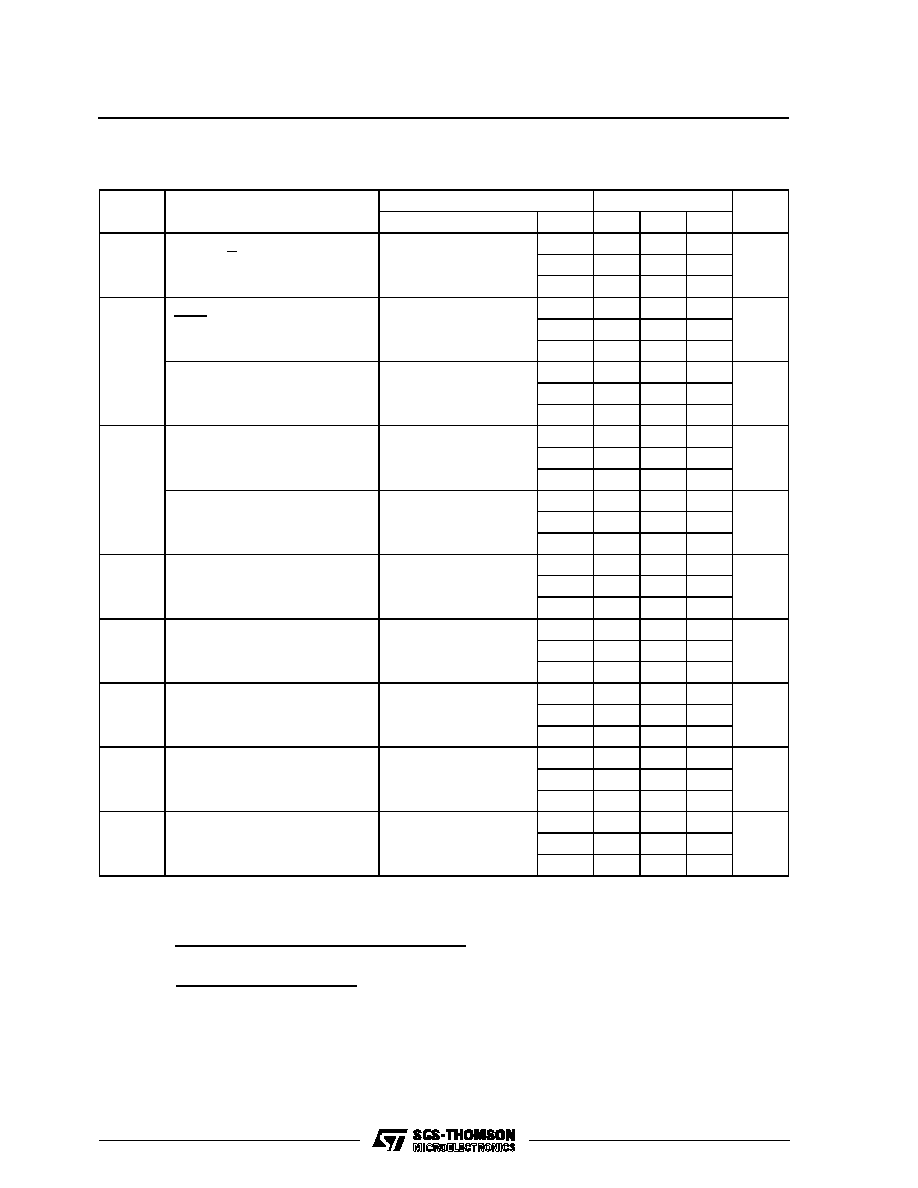
STATIC ELECTRICAL CHARACTERISTICS (over recommended operating conditions)
Test Conditions
Value
V
I
V
O
|I
O
|
V
D D
T
L o w
*
25
∞
C
T
Hi g h
*
Symbol
Parameter
(V)
(V)
(
µ
A)
(V)
Min. Max. Min. Typ. Max. Min. Max.
Unit
I
L
Quiescent
Current
HCC
Types
0/ 5
5
5
0.04
5
150
µ
A
0/10
10
10
0.04
10
300
0/15
15
20
0.04
20
600
0/20
20
100
0.08
100
3000
HCF
Types
0/ 5
5
20
0.04
20
150
0/10
10
40
0.04
40
300
0/15
15
80
0.04
80
600
V
O H
Output High
Voltage
0/ 5
0/10
0/15
< 1
< 1
< 1
5
10
15
4.95
9.95
14.95
4.95
9.95
14.95
4.95
9.95
14.95
V
V
O L
Output Low
Voltage
5/0
10/0
15/0
< 1
< 1
< 1
5
10
15
0.05
0.05
0.05
0.05
0.05
0.05
0.05
0.05
0.05
V
V
IH
Input High
Voltage
0.5/4.5
1/9
1.5/13.5
< 1
< 1
< 1
5
10
15
3.5
7
11
3.5
7
11
3.5
7
11
V
V
IL
Input Low
Voltage
4.5/0.5
9/1
13.5/1.5
< 1
< 1
< 1
5
10
15
1.5
3
4
1.5
3
4
1.5
3
4
V
I
O H
Output
Source
Current
(Source)
Q, Q, Q
CL
D
HCC
Types
0/ 5
2.5
5
≠ 2
≠ 1.6 ≠ 3.2
≠ 1.15
mA
0/ 5
4.6
5
≠ 0.64
≠ 0.51 ≠ 1
≠ 0.36
0/10
9.5
10
≠ 1.6
≠ 1.3 ≠ 2.6
≠ 0.9
0/15
13.5
15
≠ 4.2
≠ 3.4 ≠ 6.8
≠ 2.4
HCF
Types
0/ 5
2.5
5
≠ 1.53
≠ 1.36 ≠ 3.2
≠ 1.1
0/ 5
4.6
5
≠ 0.52
≠ 0.44 ≠ 1
≠ 0.36
0/10
9.5
10
≠ 1.3
≠ 1.1 ≠ 2.6
≠ 0.9
0/15
13.5
15
≠ 3.6
≠ 3.0 ≠ 6.8
≠ 2.4
I
O L
Output
Sink
Current Q
HCC
Types
0/ 5
0.4
5
2.56
2.04
4
1.44
mA
0/10
0.5
10
6.4
5.2
10.4
3.6
0/15
1.5
15
16.8
13.6
27.2
9.6
HCF
Types
0/ 5
0.4
5
2.08
1.74
4
1.43
0/10
0.5
10
5.01
4.42
10.4
3.74
0/15
1.5
15
13.6
11.56
27.2
9.52
I
O L
Output
Sink
Current
Q, Q'
CL
D
HCC
Types
0/ 5
0.4
5
0.64
0.51
1
0.36
mA
0/10
0.5
10
1.6
1.3
2.6
0.9
0/15
1.5
15
4.2
3.4
6.8
2.4
HCF
Types
0/ 5
0.4
5
0.52
0.44
1
0.36
0/10
0.5
10
1.3
1.1
2.6
0.9
0/15
1.5
15
3.6
3.0
6.8
2.4
I
IH
, I
IL
Input
Leakage
Current
HCC
Types
0/18
Any Input
18
±
0.1
±
10
≠ 5
±
0.1
±
1
µ
A
HCF
Types
0/15
15
±
0.3
±
10
≠ 5
±
0.3
±
1
C
I
Input Capacitance
Any Input
5
7.5
pF
* T
Low
= ≠ 55
∞
C for HCC device : ≠ 40
∞
C for HCF device.
* T
High
= + 125
∞
C for HCC device : + 85
∞
C for HCF device.
The Noise Margin for both "1" and "0" level is : 1V min. with V
DD
= 5V, 2V min. with V
DD
= 10V, 2.5 V min. with V
DD
= 15V.
HCC/HCF4031B
4/12
DYNAMIC ELECTRICAL CHARACTERISTICS (T
amb
= 25
∞
C, C
L
= 50pF, R
L
= 200k
,
typical temperature coefficient for all V
DD
values is 0.3%/
∞
C, all input rise and fall times = 20ns)
Test Conditions
Val ue
Symbol
Parameter
V
D D
(V)
Min.
Typ.
Max.
Unit
t
P HL
,
t
PL H
, t
PL H
Propagation Delay Time :
Clock to Q,
Clock to Q
5
250
500
ns
10
110
220
15
90
180
t
P HL
,
t
PL H
, t
PHL
Propagation Delay Time :
Clock to Q'
Clock to Q
5
190
380
ns
10
80
160
15
65
130
Clock to CL
D
5
100
200
ns
10
50
100
15
40
80
t
THL '
, t
T L H
Transition Time :
(any output, except Qt
THL
)
5
100
200
ns
10
50
100
15
40
80
t
T HL
Q,
5
50
100
ns
10
25
50
15
20
40
t
s e t u p
Data Setup Time
5
30
60
ns
10
15
30
15
10
20
t
h o ld
Data Hold Time
5
30
60
ns
10
15
30
15
10
20
t
W
Clock Pulse Width
5
120
240
ns
10
50
100
15
40
80
f
m ax
Maximum Clock Input
Frequency**
5
2
4
MHz
10
5
10
15
6
12
t
r
, t
f
Clock Input Rise or Fall Time*
5
1000
µ
s
10
1000
15
200
*
If more than one unit is cascaded in the parallel clocked application, trCL should be made less than or equal to the sum of
the propagation delay at 50pF and the transmiti on time of the output driving stage.
*
* Maximum Clock Frequency for Cascaded Units;
a) Using Delayed Clock Feature in Recirculation Mode :
fmax =
1
(n-1) CLD prop. delay + Q prop. delay + set-up time
where n = nimber of packages
b) Not Usng Delaye Clock :
fmax =
1
propagation delay + set-up time
HCC/HCF4031B
5/12

Typical Output Low (sink) Current Characteristics.
Minimum
Output Low (sink) Current Charac-
teristics.
Typical Output High (source) Current Charac-
teristics.
Minimum Output High (source) Current Charac-
teristics.
HCC/HCF4031B
6/12
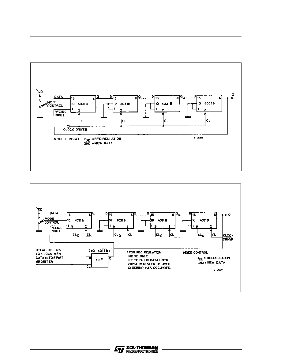
TYPICAL APPLICATIONS
CASCADING USING DIRECT CLOCKING FOR HIGH SPEED OPERATION (SEE CLOCK RISE AND FALL
TIME REQUIREMENT).
CASCADING USING DELAYED CLOCKING FOR REDUCED CLOCK DRIVE REQUIREMENTS.
HCC/HCF4031B
7/12
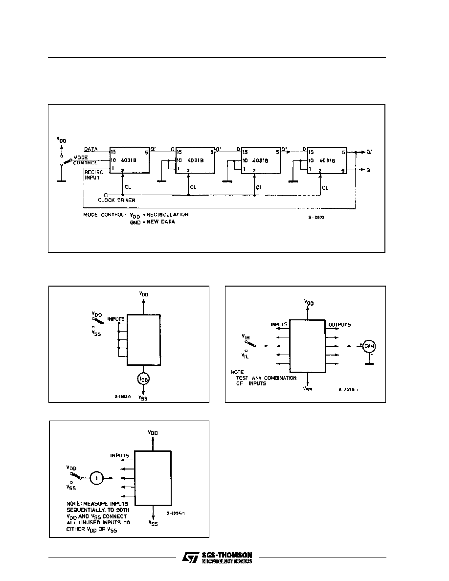
TYPICAL APPLICATIONS (continued)
CASCADING USING HALF- CLOCK-PULSE DELAYED DATA OUTPUT (Q') TO PERMIT USE OF SLOW
RISE AND FALL TIME CLOCK INPUTS.
Input Leakage Current.
Noise Immunity.
TEST CIRCUITS
Quiescent Device Current.
HCC/HCF4031B
8/12
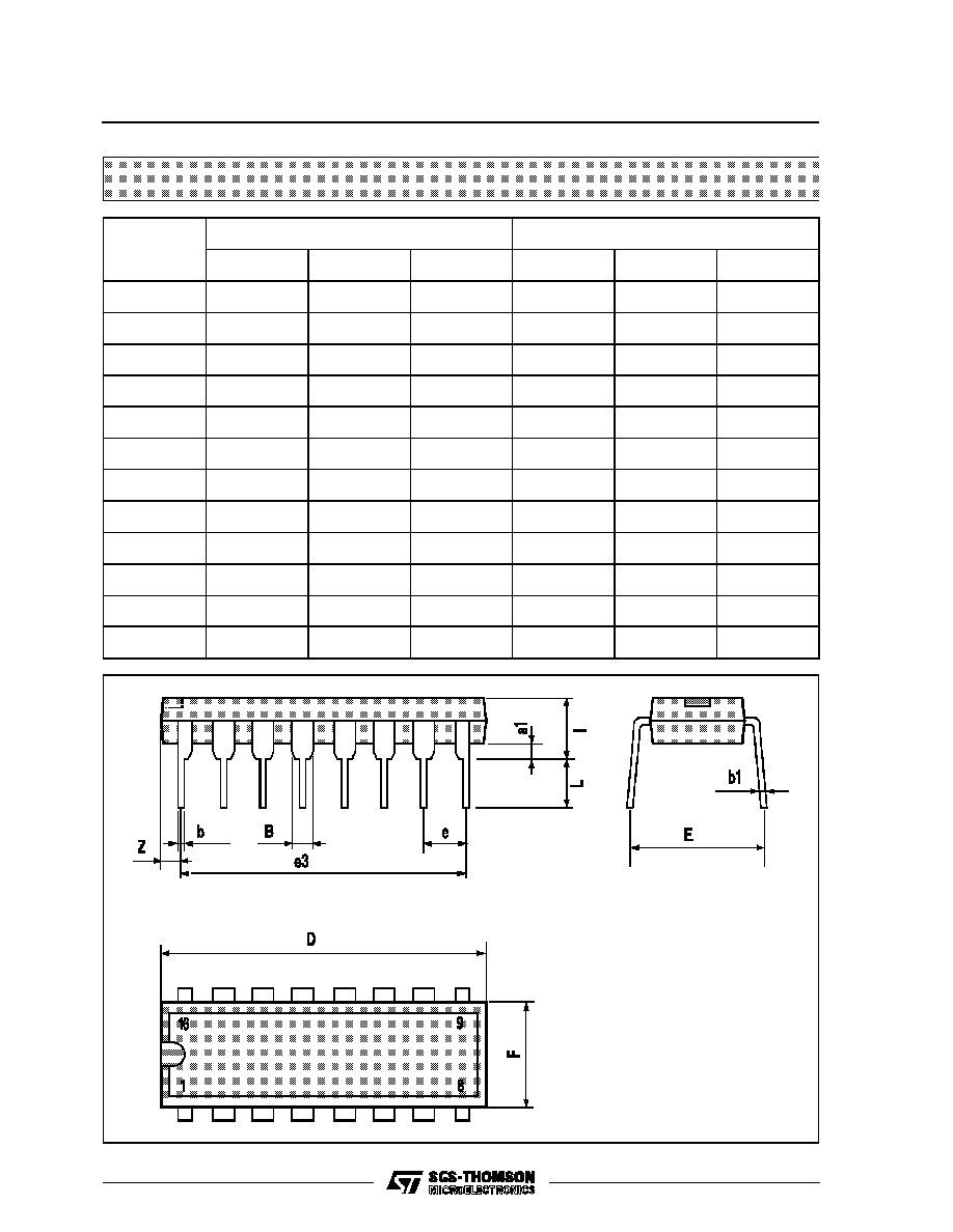
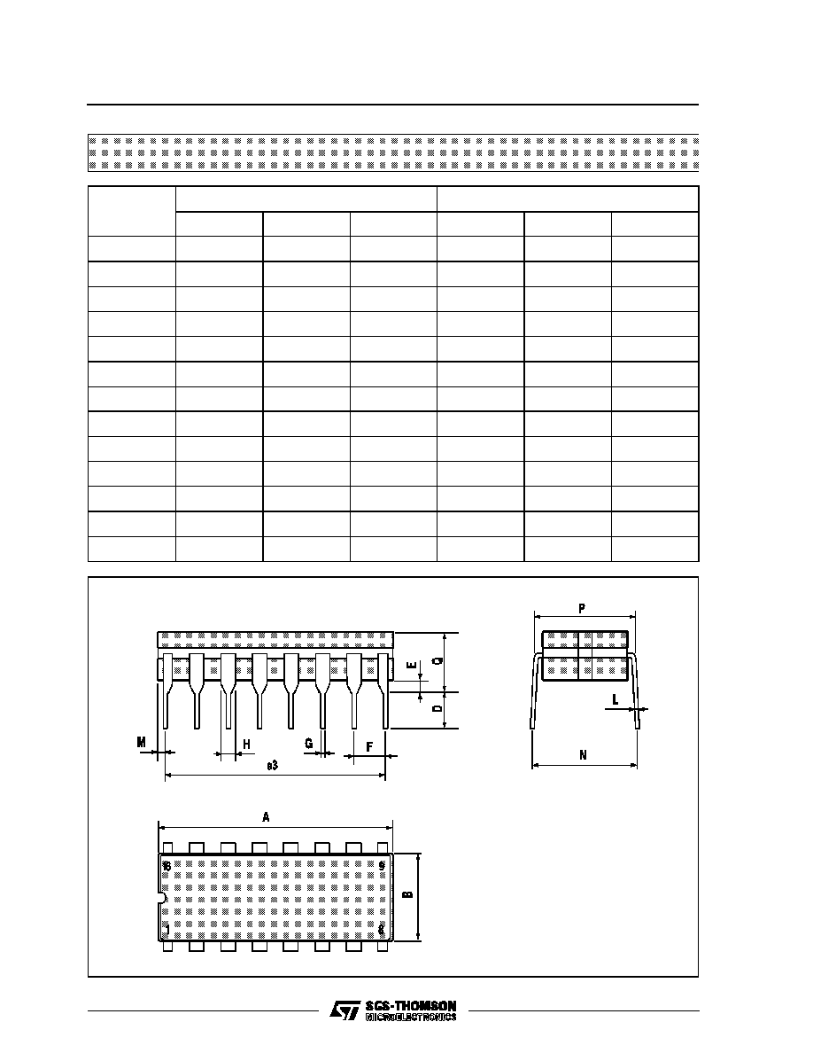
Plastic DIP16 (0.25) MECHANICAL DATA
DIM.
mm
inch
MIN.
TYP.
MAX.
MIN.
TYP.
MAX.
a1
0.51
0.020
B
0.77
1.65
0.030
0.065
b
0.5
0.020
b1
0.25
0.010
D
20
0.787
E
8.5
0.335
e
2.54
0.100
e3
17.78
0.700
F
7.1
0.280
I
5.1
0.201
L
3.3
0.130
Z
1.27
0.050
P001C
HCC/HCF4031B
9/12
Ceramic DIP16/1 MECHANICAL DATA
DIM.
mm
inch
MIN.
TYP.
MAX.
MIN.
TYP.
MAX.
A
20
0.787
B
7
0.276
D
3.3
0.130
E
0.38
0.015
e3
17.78
0.700
F
2.29
2.79
0.090
0.110
G
0.4
0.55
0.016
0.022
H
1.17
1.52
0.046
0.060
L
0.22
0.31
0.009
0.012
M
0.51
1.27
0.020
0.050
N
10.3
0.406
P
7.8
8.05
0.307
0.317
Q
5.08
0.200
P053D
HCC/HCF4031B
10/12
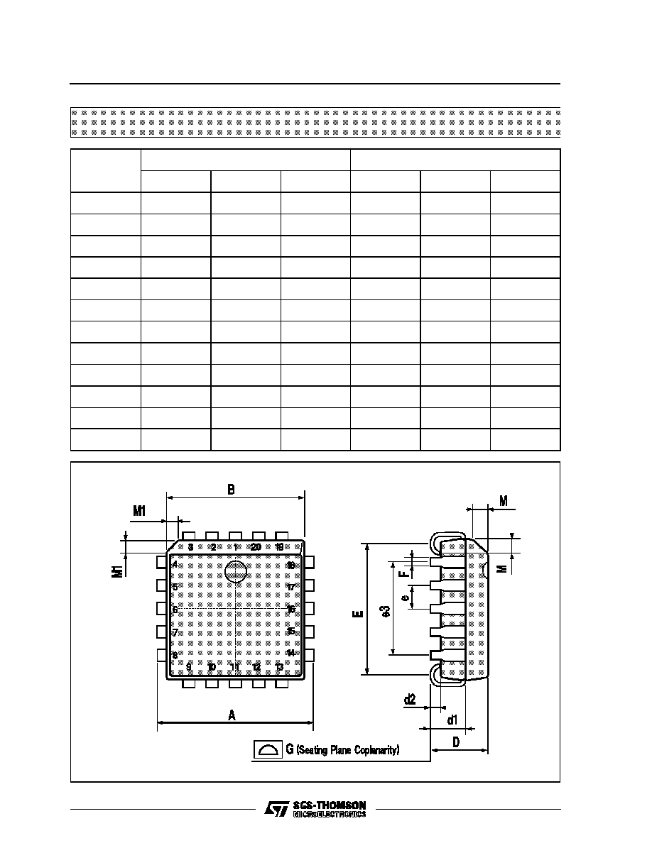
PLCC20 MECHANICAL DATA
DIM.
mm
inch
MIN.
TYP.
MAX.
MIN.
TYP.
MAX.
A
9.78
10.03
0.385
0.395
B
8.89
9.04
0.350
0.356
D
4.2
4.57
0.165
0.180
d1
2.54
0.100
d2
0.56
0.022
E
7.37
8.38
0.290
0.330
e
1.27
0.050
e3
5.08
0.200
F
0.38
0.015
G
0.101
0.004
M
1.27
0.050
M1
1.14
0.045
P027A
HCC/HCF4031B
11/12

Information furnished is believed to be accurate and reliable. However, SGS-THOMSON Microelectronics assumes no responsability for the
consequences of use of such information nor for any infringement of patents or other rights of third parties which may results from its use. No
license is granted by implication or otherwise under any patent or patent rights of SGS-THOMSON Microelectronics. Specifications mentioned
in this publication are subject to change without notice. This publication supersedes and replaces all information previously supplied.
SGS-THOMSON Microelectronics products are not authorized for use as critical components in life support devices or systems without express
written approval of SGS-THOMSON Microelectonics.
©
1994 SGS-THOMSON Microelectronics - All Rights Reserved
SGS-THOMSON Microelectronics GROUP OF COMPANIES
Australia - Brazil - France - Germany - Hong Kong - Italy - Japan - Korea - Malaysia - Malta - Morocco - The Netherlands -
Singapore - Spain - Sweden - Switzerland - Taiwan - Thailand - United Kingdom - U.S.A
HCC/HCF4031B
12/12