HCC/HCF4026B
HCC/HCF4033B
7-SEGMENT DISPLAY OUTPUTS
DECADE COUNTERS/DIVIDERS WITH DECODED
DESCRIPTION
.
COUNTER AND 7-SEGMENT DECODING IN
ONE PACKAGE
.
EASILY INTERFACED WITH 7-SEGMENT DIS-
PLAY TYPES
.
FULLY STATIC COUNTER OPERATION : DC
TO 6MHz (typ.) AT V
DD
= 10V
.
IDEAL FOR LOW-POWER DISPLAYS
.
DISPLAY ENABLE OUTPUT - 4026B
.
"RIPPLE BLANKING" AND LAMP TEST - 4033B
.
QUIESCENT CURRENT SPECIFIED TO 20V
FOR HCC DEVICE
.
STANDARDIZED
SYMMETRICAL
OUTPUT
CHARACTERISTICS
.
5V, 10V, AND 15V PARAMETRIC RATING
.
INPUT CURRENT OF 100nA AT 18V AND 25
∞
C
FOR HCC DEVICE
.
100% TESTED FOR QUIESCENT CURRENT
.
MEETS ALL REQUIREMENTS OF JEDEC TEN-
TATIVE STANDARD N
∞
13A, "STANDARD SPE-
CIFICATIONS FOR DESCRIPTION OF "B"
SERIES CMOS DEVICES"
June 1989
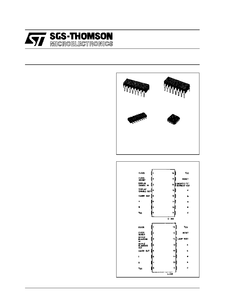
The HCC4026B/4033B (extended temperature
range) and HCF4026B/4033B (intermediate tem-
perature range) are monolithic integrated circuits,
available in 16-lead dual in-line plastic or ceramic
package
and
plastic
micro
package.
The
HCC/HCF4026B and HCC/HCF4033B each con-
sist of a 5-stage Johnson decade counter and an
output decoder which converts the Johnson code to
a 7-segment decoded output for driving one stage
in a numerical display. These devices are particu-
larly advantageous in display applications where
low power dissipation and/or low package count are
important. Inputs common to both types are
CLOCK, RESET, & CLOCK INHIBIT ; common out-
puts are CARRY OUT and the seven decoded out-
puts (a, b, c, d, e, f, g). Additional inputs and outputs
for the HCC/HCF4026B include DISPLAY ENABLE
input and DISPLAY ENABLE and UNGATED "C-
SEGMENT"
outputs. Signals peculiar
to the
HCC/HCF4033B are RIPPLE-BLANKING INPUT
AND LAMP TEST INPUT and a RIPPLE-BLANK-
ING OUTPUT. A high RESET signal clears the de-
EY
(Plastic Package)
F
(Ceramic Frit Seal Package)
C1
(Plastic Chip Carrier)
ORDER CODES :
HCC40XXBF
HCF40XXBM1
HCF40XXBEY
HCF40XXBC1
PIN CONNECTIONS
WITH; DISPLAY ENABLE 4026B
RIPPLE BLANKING 4033B
4026B
4033B
M1
(Micro Package)
1/15

cade counter to its zero count. The counter is ad-
vanced one count at the positive clock signal tran-
sition if the CLOCK INHIBIT signal is low. Counter
advancement via the clock line is inhibited when the
CLOCK INHIBIT signal is high. Antilock gating is
provided on the JOHNSON counter, thus assuring
proper counting sequence. The CARRY-OUT (C
out
)
signal completes one cycle every ten CLOCK
INPUT cycles and is used to clock the succeeding
decade directly in a multi-decade counting chain.
The seven decoded outputs (a, b, c, d, e, f, g) illumi-
nate the proper segments in a seven segment dis-
play device used for representing the decimal
numbers 0 to 9. The 7-segment outputs go high on
selection in the HCC/HCF4033B ; in the HCC/-
HCF4026B these outputs go high only when the
DISPLAY ENABLE IN is high.
HCC/HCF4026B - When the DISPLAY ENABLE IN
is low the seven decoded outputs are forced low re-
gardless of the state of the counter. Activation of the
display only when required results in significant
power savings. This system also facilitates im-
plementation of display-character multiplexing. The
CARRY OUT and UNGATED "C-SEGMENT" sig-
nals are not gated by the DISPLAY ENABLE and
therefore are available continuously. This feature is
a requirement in implementation of certain divider
functions such as divide-by-60 and divide-by-12.
HCC/HCF4033B - The HCC/HCF4033B has provi-
sions for automatic blanking of the non-significant
zeros in a multi-digit decimal number which results
in an easily readable display consistent with
normal writing practice. For example, the number
0050.07000 in an eight digit display would be dis-
played as 50.07. Zero suppression on the integer
side is obtained by connecting the RBI terminal of
the HCC/HCF4033B associated with the most sig-
nificant digit in the display to a low-level voltage and
connecting the RBO terminal of that stage to the RBI
terminal of the HCC/HCF4033B in the next-lower
significant position in the display. This procedure is
continued for each succeeding HCC/HCF4033B on
the integer side of the display. On the fraction side
of the display the RBI of the HCC/HCF4033B asso-
ciated with the least significant bit is connected to a
low-level voltage and the RBO of that HCC/-
HCF4033B is connected to the RBI terminal of the
HCC/HCF4033B in the next more-significant-bit po-
sition. Again, this procedure is continued for all
HCC/HCF4033B's on the fraction side of the dis-
play. In a purely fractional number the zero immedi-
ately preceding the decimal point can be displayed
by connecting the RBI of that stage to a high level
voltage (instead of to the RBO of the next more-sig-
nificant-stage). For example : optional zero
0.7346. Likewise, the zero in a number such as
763.0 can be displayed by connecting the RBI of the
HCC/HCF4033B associated with it to a high-level
voltage. Ripple blanking of non-significant zeros
provides an appreciable savings in display power.
The HCC/HCF4033B has a LAMP TEST input
which, when connected to a high-level voltage,
overrides normal decoder operation and enables a
check to be made on possible display malfunctions
by putting the seven outputs in the high state.
HCC/HCF4026B/4033B
2/15

FUNCTIONAL DIAGRAMS
ABSOLUTE MAXIMUM RATINGS
Symbol
Parameter
Value
Unit
V
DD
*
Supply Voltage : HCC Types
HCF Types
≠ 0.5 to + 20
≠ 0.5 to + 18
V
V
V
i
Input Voltage
≠ 0.5 to V
DD
+ 0.5
V
I
I
DC Input Current (any one input)
±
10
mA
P
tot
Total Power Dissipation (per package)
Dissipation per Output Transistor
for T
op
= Full Package-temperature Range
200
100
mW
mW
T
op
Operating Temperature : HCC Types
HCF Types
≠ 55 to + 125
≠ 40 to + 85
∞
C
∞
C
T
s tg
Storasge Temperature
≠ 65 to + 150
∞
C
RECOMMENDED OPERATING CONDITIONS
Symbol
Parameter
Value
Unit
V
DD
Supply Voltage : HCC Types
HC F Types
3 to 18
3 to 15
V
V
V
I
Input Voltage
0 to V
DD
V
T
o p
Operating Temperature : HCC Types
H CF Types
≠ 55 to + 125
≠ 40 to + 85
∞
C
∞
C
4026B
4033B
Stresses above those listed under "Absolute Maximum Ratings" may cause permanent damage to the device. This is a stress
rating only and functional operation of the device at these or any other conditions above those indicated in the operational sec-
tions of this specifi cation is not implied. Exposure to absolute maximum rating conditions for external periods may affect device
reliability.
* All voltages values are referred to V
SS
pin voltage.
HCC/HCF4026B/4033B
3/15
LOGIC DIAGRAMS
4026B
4033B
HCC/HCF4026B/4033B
4/15
4026B
4033B
TIMING DIAGRAMS
HCC/HCF4026B/4033B
5/15
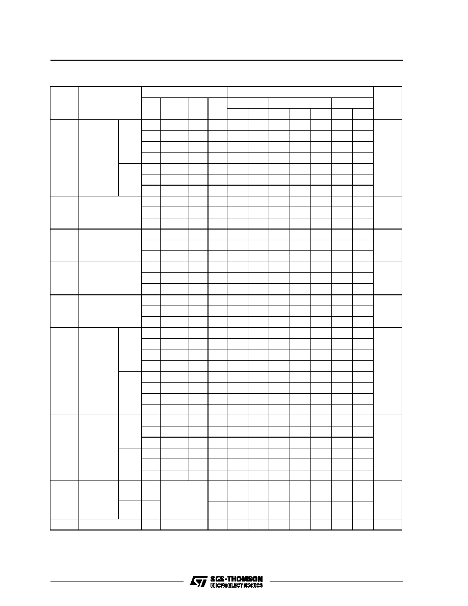
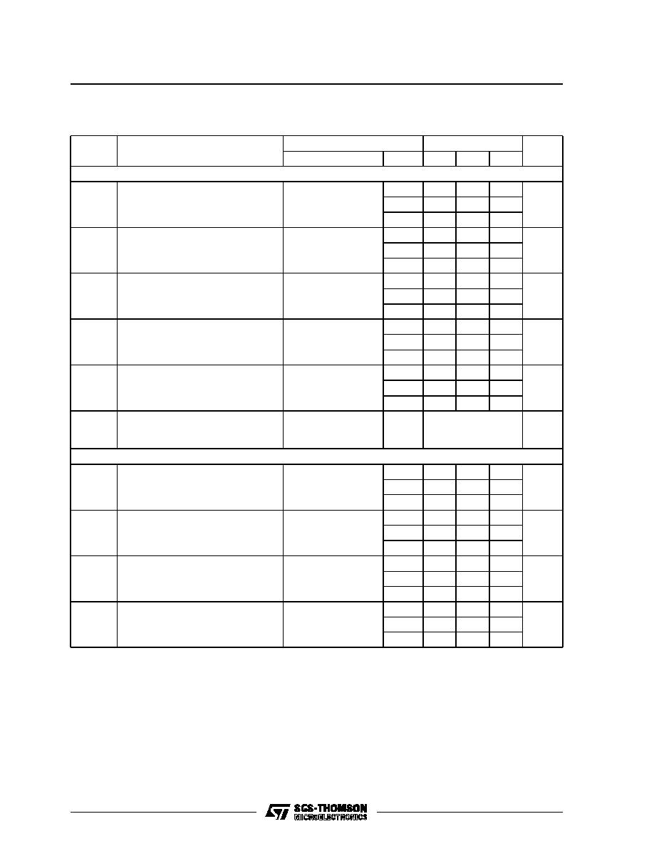
STATIC ELECTRICAL CHARACTERISTICS (over recommended operating conditions)
Test Conditions
Val ue
V
I
V
O
| I
O
|
V
DD
T
Lo w
*
25
∞
C
T
High
*
Symbol
Parameter
(V)
(V)
(
µ
A)
(V)
Min.
Max.
Min.
Typ.
Max.
Min.
Max.
Unit
I
L
Quiescent
Current
HCC
Types
0/ 5
5
5
0.04
5
150
µ
A
0/10
10
10
0.04
10
300
0/15
15
20
0.04
20
600
0/20
20
100
0.08
100
3000
HCF
Types
0/ 5
5
20
0.04
20
150
0/10
10
40
0.04
40
300
0/15
15
80
0.04
80
600
V
OH
Output High
Voltage
0/ 5
< 1
5
4.95
4.95
4.95
V
0/10
< 1
10
9.95
9.95
9.95
0/15
< 1
15
14.95
14.95
14.95
V
OL
Output Low
Voltage
5/0
< 1
5
0.05
0.05
0.05
V
10/0
< 1
10
0.05
0.05
0.05
15/0
< 1
15
0.05
0.05
0.05
V
IH
Input High
Voltage
0.5/4.5
< 1
5
3.5
3.5
3.5
V
1/9
< 1
10
7
7
7
1.5/13.5
< 1
15
11
11
11
V
IL
Input Low
Voltage
4.5/0.5
< 1
5
1.5
1.5
1.5
V
9/1
< 1
10
3
3
3
13.5/1.5
< 1
15
4
4
4
I
OH
Output
Drive
Current
HCC
Types
0/ 5
2.5
5
≠ 2
≠ 1.6 ≠ 3.2
≠ 1.15
mA
0/ 5
4.6
5
≠ 0.64
≠ 0. 51
≠ 1
≠ 0.36
0/10
9.5
10
≠ 1.6
≠ 1.3
≠ 2.6
≠ 0. 9
0/15
13.5
15
≠ 4.2
≠ 3.4
≠ 6.8
≠ 2. 4
HCF
Types
0/ 5
2.5
5
≠ 1.53
≠ 1. 36 ≠ 3.2
≠ 1. 1
0/ 5
4.6
5
≠ 0.52
≠ 0. 44
≠ 1
≠ 0.36
0/10
9.5
10
≠ 1.3
≠ 1.1
≠ 2.6
≠ 0. 9
0/15
13.5
15
≠ 3.6
≠ 3.0
≠ 6.8
≠ 2. 4
I
OL
Output
Sink
Current
HCC
Types
0/ 5
0.4
5
0.64
0.51
1
0.36
mA
0/10
0.5
10
1.6
1.3
2.6
0.9
0/15
1.5
15
4.2
3.4
6.8
2.4
HCF
Types
0/ 5
0.4
5
0.52
0.44
1
0.36
0/10
0.5
10
1.3
1.1
2.6
0.9
0/15
1.5
15
3.6
3.0
6.8
2.4
I
IH
, I
IL
Input
Leakage
Current
HCC
Types
0/18
Any Input
18
±
0. 1
±
10
≠5
±
0.1
±
1
µ
A
HCF
Types
0/15
15
±
0. 3
±
10
≠5
±
0.3
±
1
C
I
Input Capacitance
Any Input
5
7.5
pF
(*) T
Low
= ≠ 55
∞
C for HCC device : ≠ 40
∞
C for HCF device.
T
High
= + 125
∞
C for HCC device : + 85
∞
C for HCF device.
The Noise Margin for both "1" and "0" level is : 1V min. with V
DD
= 5V, 2V min. with V
DD
= 10V, 2.5V min. with V
DD
= 15V.
HCC/HCF4026B/4033B
6/15
DYNAMIC ELECTRICAL CHARACTERISTICS (T
amb
= 25
∞
C, C
L
= 50pF, R
L
= 200k
,
typical temperature coefficient for all V
DD
values is 0.3%/
∞
C, all input rise and fall times = 20ns)
Val ue
Symbol
Parameter
Test Conditions
V
D D
(V)
Min.
Typ.
Max.
Unit
CLOCKED OPERATI ON
t
P L H
, t
P HL
Propagation Delay Time
Carry Out Line
5
250
500
ns
10
100
200
15
75
150
t
P L H
, t
P HL
Propagation Delay Time
Decode Out Lines
5
350
700
ns
10
125
250
15
90
180
t
THL
, t
T L H
Transition Time
Carry Out Line
5
100
200
ns
10
50
100
15
25
50
f
CL
*
Maximum Clock Input Frequency
5
2.5
5
MHz
10
5.5
11
15
8
16
t
WC
Clock Pulse Width
5
110
270
ns
10
50
100
15
40
80
t
r
, t
f
Clock Input Rise or Fall Time
5
10
15
Unlimited
µ
s
RESET OPERATI ON
t
PL H
,
Propagation Delay Time
Carry Out Line
5
275
550
ns
10
120
240
15
80
160
t
P L H
, t
P HL
Propagation Delay Time
Decode Out Lines
5
300
600
ns
10
125
250
15
90
180
t
WR
Reset Pulse Width
5
100
120
ns
10
50
100
15
25
50
t
r e m
Reset Removal Time
5
0
30
ns
10
0
15
15
0
10
* Measured with respect to carry output line.
HCC/HCF4026B/4033B
7/15
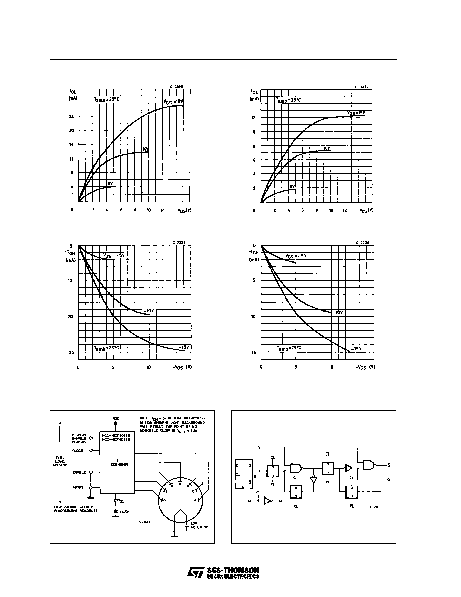
Typical Output Low (sink) Current.
Minimum Output Low (sink) Current Characteristics.
Typical Output High (source) Current Charac-
teristics.
Minimum Output High (source) Current Charac-
teristics.
TYPICAL APPLICATIONS
Interfacing with Filament Fluorescent Display.
Detail of Typical Flip-flop Stage for Both Types.
HCC/HCF4026B/4033B
8/15

Interfacing with LED Displays (display common
anode).
Interfacing with NIXIE Tube.
(Display Common Cathode).
TYPICAL APPLICATIONS (continued)
HCC/HCF4026B/4033B
9/15
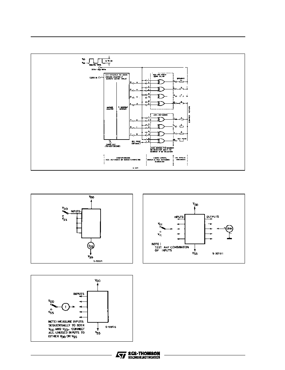
TEST CIRCUITS
Quiescent Device Current.
Input Current.
Input Voltage.
Interfacing with Liquid Cristal Displays.
HCC/HCF4026B/4033B
10/15

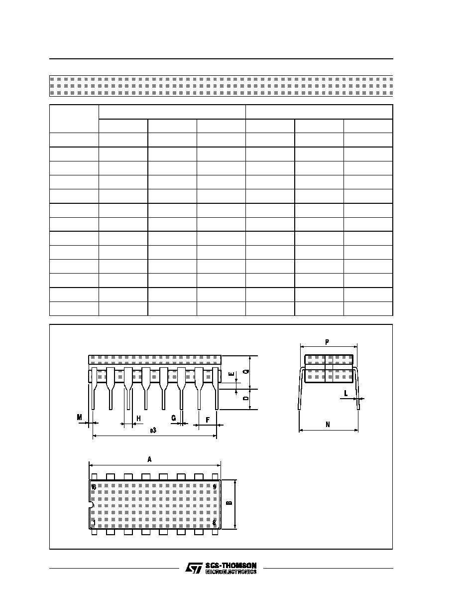
Plastic DIP16 (0.25) MECHANICAL DATA
DIM.
mm
inch
MIN.
TYP.
MAX.
MIN.
TYP.
MAX.
a1
0.51
0.020
B
0.77
1.65
0.030
0.065
b
0.5
0.020
b1
0.25
0.010
D
20
0.787
E
8.5
0.335
e
2.54
0.100
e3
17.78
0.700
F
7.1
0.280
I
5.1
0.201
L
3.3
0.130
Z
1.27
0.050
P001C
HCC/HCF4026B/4033B
11/15
Ceramic DIP16/1 MECHANICAL DATA
DIM.
mm
inch
MIN.
TYP.
MAX.
MIN.
TYP.
MAX.
A
20
0.787
B
7
0.276
D
3.3
0.130
E
0.38
0.015
e3
17.78
0.700
F
2.29
2.79
0.090
0.110
G
0.4
0.55
0.016
0.022
H
1.17
1.52
0.046
0.060
L
0.22
0.31
0.009
0.012
M
0.51
1.27
0.020
0.050
N
10.3
0.406
P
7.8
8.05
0.307
0.317
Q
5.08
0.200
P053D
HCC/HCF4026B/4033B
12/15
SO16 (Narrow) MECHANICAL DATA
DIM.
mm
inch
MIN.
TYP.
MAX.
MIN.
TYP.
MAX.
A
1.75
0.068
a1
0.1
0.2
0.004
0.007
a2
1.65
0.064
b
0.35
0.46
0.013
0.018
b1
0.19
0.25
0.007
0.010
C
0.5
0.019
c1
45
∞
(typ.)
D
9.8
10
0.385
0.393
E
5.8
6.2
0.228
0.244
e
1.27
0.050
e3
8.89
0.350
F
3.8
4.0
0.149
0.157
G
4.6
5.3
0.181
0.208
L
0.5
1.27
0.019
0.050
M
0.62
0.024
S
8
∞
(max.)
P013H
HCC/HCF4026B/4033B
13/15
PLCC20 MECHANICAL DATA
DIM.
mm
inch
MIN.
TYP.
MAX.
MIN.
TYP.
MAX.
A
9.78
10.03
0.385
0.395
B
8.89
9.04
0.350
0.356
D
4.2
4.57
0.165
0.180
d1
2.54
0.100
d2
0.56
0.022
E
7.37
8.38
0.290
0.330
e
1.27
0.050
e3
5.08
0.200
F
0.38
0.015
G
0.101
0.004
M
1.27
0.050
M1
1.14
0.045
P027A
HCC/HCF4026B/4033B
14/15
Information furnished is believed to be accurate and reliable. However, SGS-THOMSON Microelectronics assumes no responsability for the
consequences of use of such information nor for any infringement of patents or other rights of third parties which may results from its use. No
license is granted by implication or otherwise under any patent or patent rights of SGS-THOMSON Microelectronics. Specifications mentioned
in this publication are subject to change without notice. This publication supersedes and replaces all information previously supplied.
SGS-THOMSON Microelectronics products are not authorized for use as critical components in life support devices or systems without express
written approval of SGS-THOMSON Microelectonics.
©
1994 SGS-THOMSON Microelectronics - All Rights Reserved
SGS-THOMSON Microelectronics GROUP OF COMPANIES
Australia - Brazil - France - Germany - Hong Kong - Italy - Japan - Korea - Malaysia - Malta - Morocco - The Netherlands -
Singapore - Spain - Sweden - Switzerland - Taiwan - Thailand - United Kingdom - U.S.A
HCC/HCF4026B/4033B
15/15