 | –≠–ª–µ–∫—Ç—Ä–æ–Ω–Ω—ã–π –∫–æ–º–ø–æ–Ω–µ–Ω—Ç: HCC4042BF | –°–∫–∞—á–∞—Ç—å:  PDF PDF  ZIP ZIP |

HCC/HCF4042B
June 1989
QUAD CLOCKED "D" LATCH
.
CLOCK POLARITY CONTROL
.
Q AND Q OUTPUTS
.
COMMON CLOCK
.
LOW POWER TTL COMPATIBLE
.
STANDARDIZED
SYMMETRICAL
OUTPUT
CHARACTERISTICS
.
QUIESCENT CURRENT SPECIFIED TO 20V
FOR HCC DEVICE
.
5V, 10V, AND 15V PARAMETRIC RATINGS
.
INPUT CURRENT OF 100nA AT 18V AND 25
∞
C
FOR HCC DEVICE
.
100% TESTED FOR QUIESCENT CURRENT
.
MEETS ALL REQUIREMENTS OF JEDEC TEN-
TATIVE STANDARD N
∞
13A, "STANDARD SPE-
CIFICATIONS FOR DESCRIPTION OF "B"
SERIES CMOS DEVICES"
DESCRIPTION
The HCC4042B (extended temperature range) and
HCF4042B (intermediate temperature range) are
monolithic integrated circuit, available in 16-lead
dual in-line plastic or ceramic package and plastic
micro package.
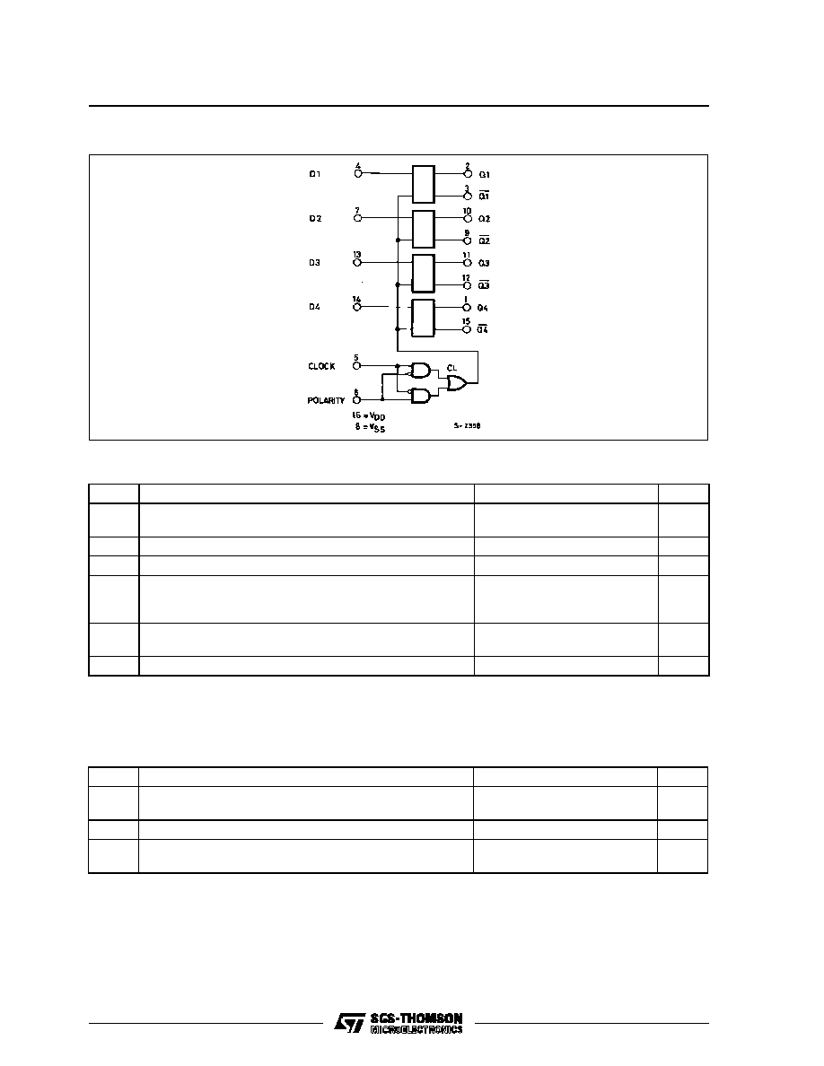
The HCC/HCF4042B types contain four latch cir-
cuits, each strobed by a common clock. Com-
plementary buffered outputs are available from
each circuit. The impedance of the n- and p-channel
output devices is balanced and all outputs are elec-
trically identical.
Information present at the data input is transferred
to outputs Q and Q during the CLOCK level which
is programmed by the POLARITY input. For PO-
LARITY = 0 the transfer occurs during the 0 CLOCK
level and for POLARITY = 1 the transfer occurs dur-
ing the 1 CLOCK level. The outputs follow the data
input providing the CLOCK and POLARITY levels
defined above are present. When a CLOCK transi-
tion occurs (positive for POLARITY = 0 and negative
for POLARITY = 1) the information present at the
input during the CLOCK transition is retained at the
outputs until an opposite CLOCK transition occurs.
EY
(Plastic Package)
F
(Ceramic Package)
M1
(Micro Package)
C1
(Plastic Chip Carrier)
ORDER CODES :
HCC4042BF
HCF4042BM1
HCF4042BEY
HCF4042BC1
PIN CONNECTIONS
1/13
ABSOLUTE MAXIMUM RATINGS
Symbol
Parameter
Value
Unit
V
DD
*
Supply Voltage : HC C Types
H C F Types
≠ 0.5 to + 20
≠ 0.5 to + 18
V
V
V
i
Input Voltage
≠ 0.5 to V
DD
+ 0.5
V
I
I
DC Input Current (any one input)
±
10
mA
P
t o t
Total Power Dissipation (per package)
Dissipation per Output Transistor
for T
o p
= Full Package-temperature Range
200
100
mW
mW
T
o p
Operating Temperature : HCC Types
H CF Types
≠ 55 to + 125
≠ 40 to + 85
∞
C
∞
C
T
s t g
Storage Temperature
≠ 65 to + 150
∞
C
Stresses above those listed under "Absolute Maximum Ratings" may cause permanent damage to the device. This is a stress
rating only and functional operation of the device at these or any other conditions above those indicated in the operational sections
of this specification is not implied. Exposure to absolute maximum rating conditions for external periods may affect device reliability.
* All voltage values are referred to V
SS
pin voltage.
FUNCTIONAL DIAGRAM
RECOMMENDED OPERATING CONDITIONS
Symbol
Parameter
Val ue
Unit
V
DD
Supply Voltage
:
HCC Types
HCF Types
3 t o 18
3 t o 15
V
V
V
I
Input Voltage
0 to V
DD
V
T
op
Operating Temperature : HCC Types
HCF Types
≠ 55 to + 125
≠ 40 to + 85
∞
C
∞
C
HCC/HCF4042B
2/13
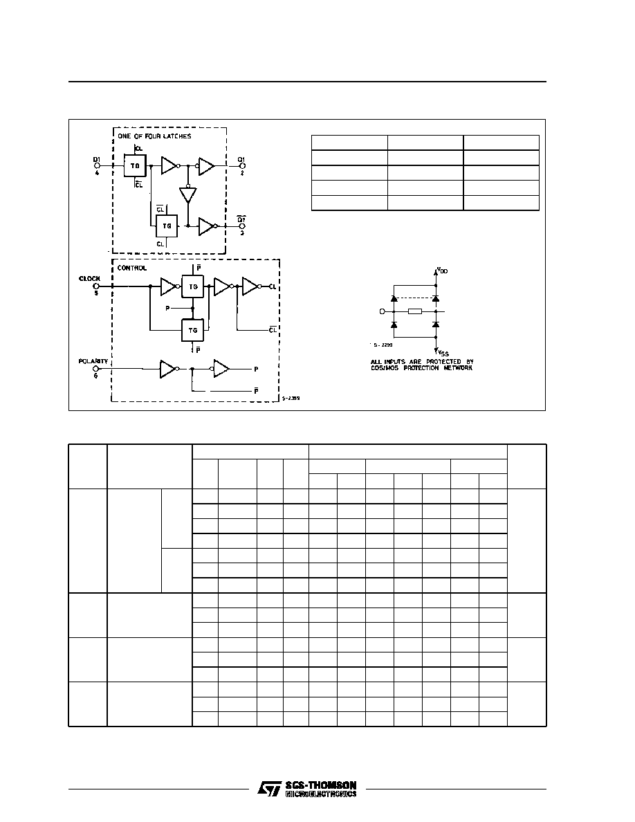
LOGIC BLOCK DIAGRAM AND TRUTH TABLE
Clock
Polarity
Q
0
0
D
__
/
__
0
Latch
1
1
D
__
\__
1
Latch
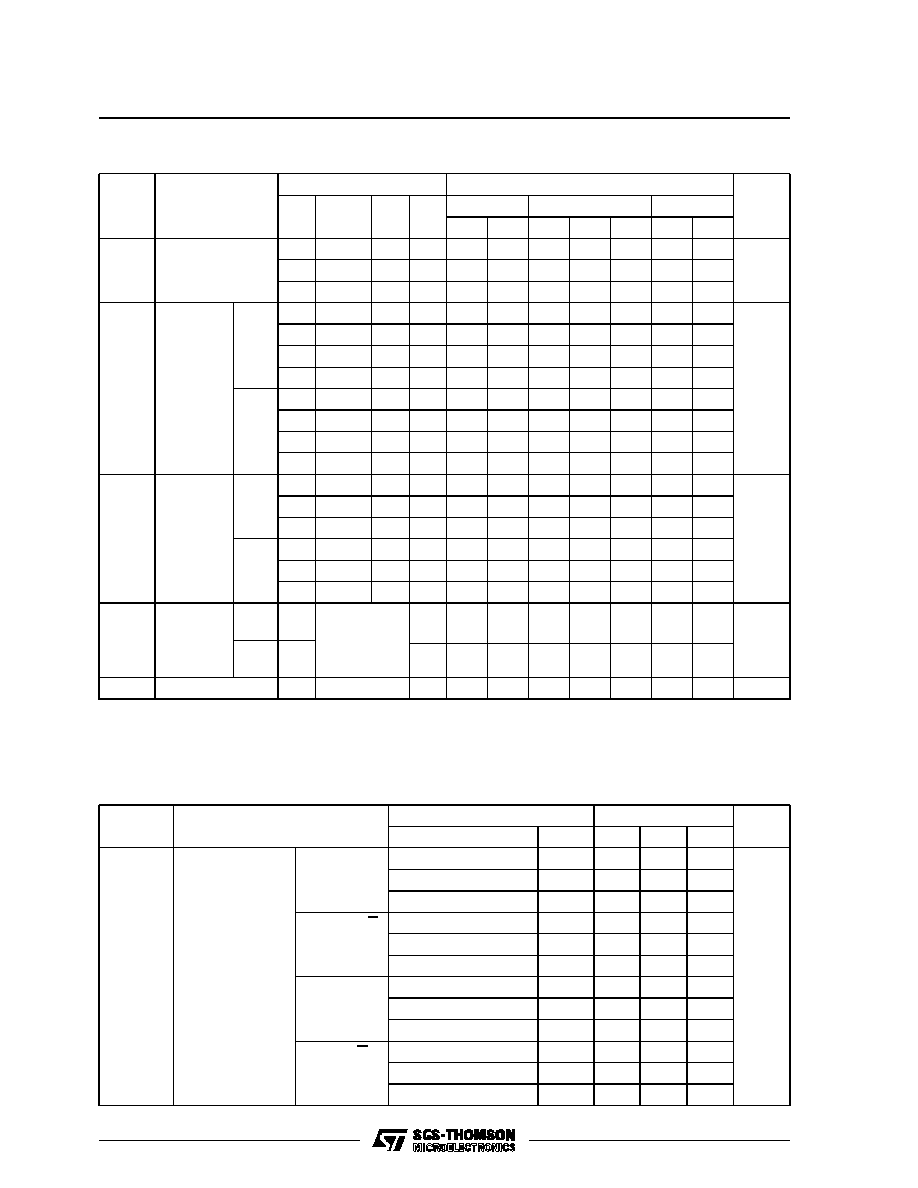
STATIC ELECTRICAL CHARACTERISTICS (over recommended operating conditions)
Test Conditions
Value
V
I
V
O
|I
O
|
V
D D
T
L o w
*
25
∞
C
T
Hi g h
*
Symbol
Parameter
(V)
(V)
(
µ
A)
(V)
Min. Max. Min. Typ. Max. Min. Max.
Unit
I
L
Quiescent
Current
HCC
Types
0/ 5
5
1
0.02
1
30
µ
A
0/10
10
2
0.02
2
60
0/15
15
4
0.02
4
120
0/20
20
20
0.04
20
600
HCF
Types
0/5
5
4
0.02
4
30
0/10
10
8
0.02
8
60
0/15
15
16
0.02
16
120
V
O H
Output High
Voltage
0/ 5
< 1
5
4.95
4.95
4.95
V
0/10
< 1
10
9.95
9.95
9.95
0/15
< 1
15
14.95
14.95
14.95
V
O L
Output Low
Voltage
5/0
< 1
5
0.05
0.05
0.05
V
10/0
< 1
10
0.05
0.05
0.05
15/0
< 1
15
0.05
0.05
0.05
V
IH
Input High
Voltage
0.5/4.5
< 1
5
3.5
3.5
3.5
V
1/9
< 1
10
7
7
7
1.5/13.5
< 1
15
11
11
11
* T
Lo w
= ≠ 55
∞
C for HCC device : ≠ 40
∞
C for HCF device.
* T
High
= + 125
∞
C for HCC device : + 85
∞
C for HCF device.
The Noise Margin for both "1" and " 0" level is : 1V min. with V
DD
= 5V, 2V min. with V
DD
= 10V, 2.5V min. with V
DD
= 15V.
HCC/HCF4042B
3/13
DYNAMIC ELECTRICAL CHARACTERISTICS (T
amb
= 25
∞
C, C
L
= 50pF, R
L
= 200k
,
typical temperature coefficient for all V
DD
values is 0.3%/
∞
C, all input rise and fall times = 20ns)
Test Conditions
Val ue
Symbol
Parameter
V
D D
( V ) Min.
Typ.
Max.
Unit
t
PL H
, t
PHL
Propagation Delay
Time
Data in to Q
5
110
220
ns
10
55
110
15
40
80
Data in to Q
5
150
300
10
75
150
15
50
100
Clock to Q
5
225
450
10
100
200
15
80
160
Clock to Q
5
250
500
10
115
230
15
90
180
STATIC ELECTRICAL CHARACTERISTICS (continued)
Test Conditions
Value
V
I
V
O
|I
O
|
V
D D
T
L o w
*
25
∞
C
T
Hi g h
*
Symbol
Parameter
(V)
(V)
(
µ
A)
(V)
Min. Max. Min. Typ. Max. Min. Max.
Unit
V
IL
Input Low
Voltage
4.5/0.5
< 1
5
1.5
1.5
1.5
V
9/1
< 1
10
3
3
3
13.5/1.5
< 1
15
4
4
4
I
O H
Output
Drive
Current
HCC
Types
0/ 5
2.5
5
≠ 2
≠ 1.6 ≠ 3.2
≠ 1.15
mA
0/ 5
4.6
5
≠ 0.64
≠ 0.51 ≠ 1
≠ 0.36
0/10
9.5
10
≠ 1.6
≠ 1.3 ≠ 2.6
≠ 0.9
0/15
13.5
15
≠ 4.2
≠ 3.4 ≠ 6.8
≠ 2.4
HCF
Types
0/ 5
2.5
5
≠ 1.53
≠ 1.36 ≠ 3.2
≠ 1.1
0/ 5
4.6
5
≠ 0.52
≠ 0.44 ≠ 1
≠ 0.36
0/10
9.5
10
≠ 1.3
≠ 1.1 ≠ 2.6
≠ 0.9
0/15
13.5
15
≠ 3.6
≠ 3.0 ≠ 6.8
≠ 2.4
I
O L
Output
Sink
Current
HCC
Types
0/ 5
0.4
5
0.64
0.51
1
0.36
mA
0/10
0.5
10
1.6
1.3
2.6
0.9
0/15
1.5
15
4.2
3.4
6.8
2.4
HCF
Types
0/ 5
0.4
5
0.52
0.44
1
0.36
0/10
0.5
10
1.3
1.1
2.6
0.9
0/15
1.5
15
3.6
3.0
6.8
2.4
I
IH
, I
IL
Input
leakage
Curent
HCC
Types
0/18
Any Input
18
±
0.1
±
10
-5
±
0.1
±
1
µ
A
HCF
Types
0/15
15
±
0.3
±
10
-5
±
0.3
±
1
C
I
Input Capacitance
Any Input
5
7.5
pF
* T
Low
= ≠ 55
∞
C for HCC device : ≠ 40
∞
C for HCF device.
* T
High
= + 125
∞
C for HCC device : + 85
∞
C for HCF device.
The Noise Margin for both "1" and "0" level is : 1V min. with V
DD
= 5V, 2V min. with V
DD
= 10V, 2.5V min. with V
DD
= 15V.
HCC/HCF4042B
4/13
DYNAMIC ELECTRICAL CHARACTERISTICS (continued)
Test Conditions
Val ue
Symbol
Parameter
V
D D
( V ) Min.
Typ.
Max.
Unit
t
T HL
, t
TL H
Transition Time
5
100
200
ns
10
50
100
15
40
80
t
W
Clock Pulse Width
5
200
100
ns
10
100
50
15
60
30
t
s e t u p
Setup Time
5
50
0
ns
10
30
0
15
25
0
t
h o ld
Hold Time
5
120
60
ns
10
60
30
15
50
25
t
r
,t
f
Clock Input Rise or Fall Time
5
Not Rise or Fall
Time Sensitive
µ
s
10
15
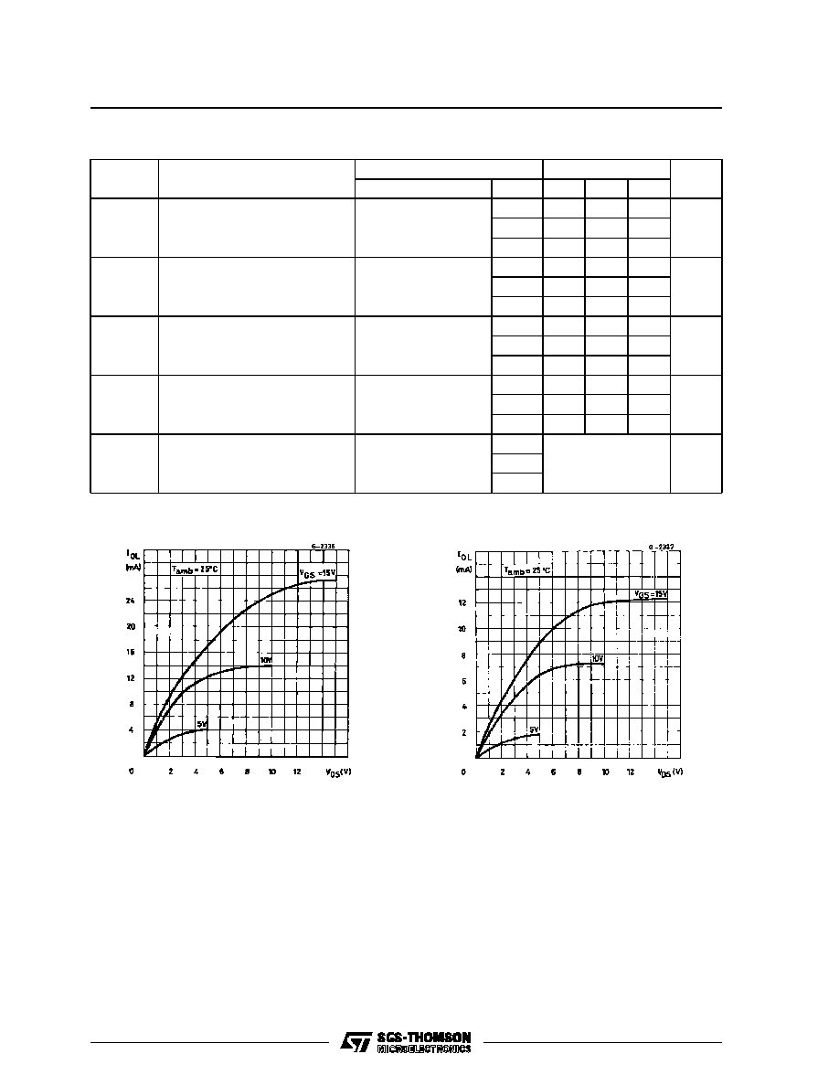
Typical Output Low (sink) Current Characteristics.
Minimum Output Low (sink) Current
Characteristics.
HCC/HCF4042B
5/13