 | –≠–ª–µ–∫—Ç—Ä–æ–Ω–Ω—ã–π –∫–æ–º–ø–æ–Ω–µ–Ω—Ç: HCC4051 | –°–∫–∞—á–∞—Ç—å:  PDF PDF  ZIP ZIP |
HCC4051B/52B/53B
HCF4051B/52B/53B
ANALOG MULTIPLEXERS-DEMULTIPLEXERS
.
QUIESCENT CURRENT SPECIFIED TO 20V
FOR HCC DEVICE
.
LOW "ON" RESISTANCE : 125
(typ.) OVER
15V p.p. SIGNAL-INPUT RANGE FOR V
DD
-
V
EE
= 15V
.
HIGH "OFF" RESISTANCE : CHANNEL LEAK-
AGE
±
100pA (typ.) V
DD
≠ V
EE
= 18V
.
BINARY ADDRESS DECODING ON CHIP
.
VERY LOW QUIESCENT POWER DISSIPA-
TION UNDER ALL DIGITAL CONTROL INPUT
AND SUPPLY CONDITIONS : 0.2
µ
W (typ.),
V
DD
≠ V
SS
= V
DD
≠ V
EE
= 10V
.
MATCHED SWITCH CHARACTERISTICS :
R
ON
= 5
(typ.) for V
DD
≠ V
EE
= 15V
.
WIDE RANGE OF DIGITAL AND ANALOG SIG-
NAL LEVELS : DIGITAL 3 TO 20V, ANALOG TO
20V p.p.
.
5V, 10V, AND 15V PARAMETRIC RATINGS
.
INPUT CURRENT OF 100mA AT 18V AND
25
∞
C FOR HCC DEVICE
.
100% TESTED FOR QUIESCENT CURRENT
.
MEETS ALL REQUIREMENTS OF JEDEC TEN-
TATIVE STANDARD N
o
13A, "STANDARD
SPECIFICATIONS FOR DESCRIPTION OF "B"
SERIES CMOS DEVICES"
4051B - SINGLE 8-CHANNEL
4052B - DIFFERENTIAL 4-CHANNEL
4053B - TRIPLE 2-CHANNEL
June 1989
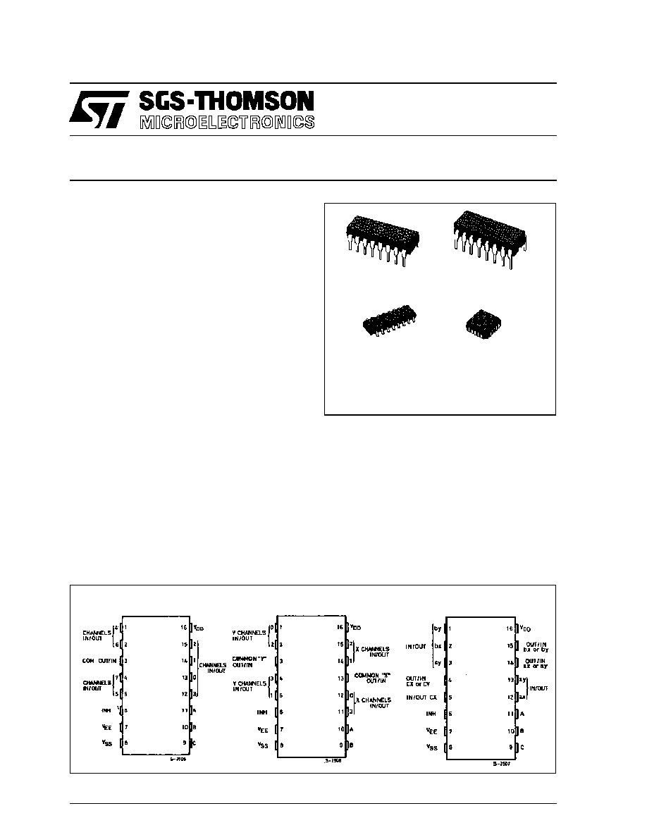
The HCC 4051B, 4052B and 4053B (extended tem-
perature range) and HCF4051B, 4052B and 4053B
(intermediate temperature range) are monolithic in-
tegrated circuits, available in 16-lead dual in-line
plastic or ceramic package and plastic micropack-
age.
HCC/HCF4051B,
HCC/HCF4052B,
and
HCC/HCF4053B
analog
multiplexers/demulti-
plexers are digitally controlled analog switches hav-
ing low ON impedance and very low OFF leakage
PIN CONNECTIONS
EY
(Plastic Package)
F
(Ceramic Frit Seal Package)
M1
(Micro Package)
C1
(Plastic Chip Carrier)
ORDER CODES :
HCC40XXBF
HCF40XXBM1
HCF40XXBEY
HCF40XXBC1
4051B
4052B
4053B
DESCRIPTION
1/17

FUNCTIONAL DIAGRAMS AND TRUTH TABLES
current. These multiplexer circuits dissipate ex-
tremely low quiescent power over the full V
DD
≠ V
SS
and V
DD
≠ V
EE
supply-voltage ranges, independent
of the logic state of the control signals. When a-logic
"1" is present at the inhibit input terminal all channel
are off. The HCC/HCF4051B is a single 8-channel
multiplexer having three binary control inputs, A, B,
and C, and an inhibit input. The three binary signals
select 1 of 8 channels to be turned on, and connect
one
of
the
8
inputs
to
the
output.
The
HCC/HCF4052B is a differential 4-channel multi-
plexer having two binary control inputs, A and B, and
an inhibit input. The two binary input signals select
1 of 4 pairs of channels to be turned on and connect
the
analog
inputs
to
the
outputs.
The
HCC/HCF4053B is a triple 2-channel multiplexer
having three separate digital control inputs, A, B,
and C, and an inhibit input. Each control input se-
lects one of a pair of channels which are connected
in a singlepole double-throw configuration.
Input States
Inhibit
C
B
A
"On" Channel (S)
0
0
0
0
0
0
0
0
1
1
0
0
1
0
2
0
0
1
1
3
0
1
0
0
4
0
1
0
1
5
0
1
1
0
6
0
1
1
1
7
1
X
X
X
None
4052B
Inhibit
B
A
0
0
0
0x, 0y
0
0
1
1x, 1y
0
1
0
2x, 2y
0
1
1
3x, 3y
1
X
X
None
4051B
HCC/HCF4051B/52B/53B
2/17
ABSOLUTE MAXIMUM RATINGS
Symbol
Parameter
Value
Unit
V
DD
*
Supply Voltage : HC C Types
H C F Types
≠ 0.5 to + 20
≠ 0.5 to + 18
V
V
V
i
Input Voltage
≠ 0.5 to V
DD
+ 0.5
V
I
I
DC Input Current (any one input)
±
10
mA
P
t o t
Total Power Dissipation (per package)
Dissipation per Output Transistor
for T
o p
= Full Package-temperature Range
200
100
mW
mW
T
o p
Operating Temperature : HCC Types
H CF Types
≠ 55 to + 125
≠ 40 to + 85
∞
C
∞
C
T
s t g
Storage Temperature
≠ 65 to + 150
∞
C
RECOMMENDED OPERATING CONDITIONS
Symbol
Parameter
Value
Unit
V
DD
Supply Voltage : HC C Types
H C F Types
3 to 18
3 to 15
V
V
V
I
Input Voltage
0 to V
DD
V
T
o p
Operating Temperature : H CC Types
H C F Types
≠ 55 to + 125
≠ 40 to + 85
∞
C
∞
C
Stresses above those listed under "Absolute Maximum Ratings" may cause permanent damage to the device. This is a stress
rating only and functional operation of the device at these or any other conditions above those indicated in the operational sec-
tions of this specifi cation is not implied. Exposure to absolute maximum rating conditions for external periods may affect device
reliability.
* All voltage values are referred to V
SS
pin voltage.
Inhibit
A or B
or C
0
0
ax or bx or cx
0
1
ay or by or cy
1
X
None
FUNCTIONAL DIAGRAMS AND TRUTH TABLES (continued)
4053
X = Don't care.
HCC/HCF4051B/52B/53B
3/17
STATIC ELECTRICAL CHARACTERISTICS (over recommended operating conditions)
Test Conditions
Val ue
V
IS
V
EE
V
SS
V
DD
T
Lo w
*
2 5
∞
C
T
High
*
Symbol
Parameter
(V)
(V)
(V)
(V)
Min.
Max.
Min.
Typ.
Max.
Min.
Max.
Unit
I
L
Quiescent
Device
Current
HCC
Types
5
5
0.04
5
150
µ
A
10
10
0.04
10
300
15
20
0.04
20
600
20
100
0.08
100
3000
HCF
Types
5
20
0.04
20
150
10
40
0.04
40
300
15
80
0.04
80
600
SWITCH
ON
Resistance
HCC
Types
0
V
I
V
DD
0
0
5
880
470
1050
1200
10
310
180
400
580
15
220
125
280
400
HCF
Types
0
V
I
V
DD
0
0
5
880
470
1050
1200
10
330
180
400
520
15
230
125
280
360
ON
Resistance
R
ON
(between any 2
channels)
0
0
5
10
10
10
15
5
OFF (
∑
)
Channel
Leakage
Current
Any
Channel
OFF
HCC
Types
0
0
18
100
±
0.1
100
1000
nA
All
Channels
OFF
(common
OUT/IN)
HCC
Types
0
0
18
100
±
0.1
100
1000
nA
Any
Channel
OFF
HCF
Types
0
0
15
300
±
0.1
300
1000
nA
All
Channels
OFF
(common
OUT/IN)
HCF
Types
0
0
15
300
±
0.1
300
1000
nA
C
Capaci-
tance
Input
5
pF
Output 4051
≠ 5
≠ 5
5
30
Output 4052
18
Output 4053
9
Feedthrough
0.2
CONTROL (Address or Inhibit)
V
IL
Input Low Voltage
= V
DD
Thru
1K
V
EE
= V
SS
R
L
= 1K
to V
SS
I
IS
< 2
µ
A
(on all off
channels)
5
1.5
1.5
1.5
V
10
3
3
3
15
4
4
4
V
IH
Input High Voltage
5
3.5
3.5
3.5
V
10
7
7
7
15
11
11
11
I
IH
, I
IL
Input
Leakage
Current
HCC
Types
V
I
= 0/18V
18
±
0. 1
±
10
≠3
±
0.1
±
1
µ
A
HCF
Types
V
I
= 0/15V
15
±
0. 3
±
10
≠3
±
0.3
±
1
C
I
Input Capacitance
Any Address or Inhibit
Input
5
7.5
pF
(
∑
) Determined by minimum feasible leakage measurement for automatic testing.
(*) T
Low
= ≠ 55
∞
C for HCC device : ≠ 40
∞
C for HCF device.
(*) T
High
= + 125
∞
C for HCC device : + 85
∞
C for HCF device.
HCC/HCF4051B/52B/53B
4/17
DYNAMIC ELECTRICAL CHARACTERISTICS
(T
am b
= 25
∞
C, C
L
= 50pF all input square wave rise and fall time = 20ns)
Test Conditions
Val ue
Parameter
V
EE
(V)
R
L
(k
)
f
i
(kHz)
V
IS
(V)
V
S S
(V)
V
DD
(V)
Typ. Max.
Unit
SWI TCH
t
p d
Propagation Delay Time
(signal input to output)
200
10 V
_I
__
I_
5
30
30
ns
10
15
60
15
11
20
Frequency Response
Channel "ON" (sine wave
input)
= V
S S
1
5 (
∑
)
10
V
o
at Common
OUT/IN
4053B
30
MHz
4052B
25
4051B
20
V
o
at 20 Log
= ≠ 3dB
__
V
I
V
o
at any Channel
60
Feedthrough (all channels
OFF)
= V
S S
1
5 (
∑
)
10
V
o
at Common
OUT/IN
4053
8
MHz
4052
10
4051
12
V
o
at 20 Log
= ≠ 40dB
__
V
I
V
o
at any Channel
8
Frequency Signal Crosstalk
Between any 2 Channels
3
V
o
at 20 Log
= ≠ 40dB
__
V
I
= V
S S
1
5 (
∑
)
10
Between Sections
4052B only
measured
o n
common
6
MHz
MHz
measured
on any
channel
10
Between any 2
Sections 4053B
only
in Pin 2
out Pin 14
2.5
in Pin 15
out Pin 14
6
Sine Wave Distortion
f
i s
= 1kHz Sine Wave
= V
S S
10
1
2 (
∑
)
5
0.3
%
10
1
3 (
∑
)
10
0.2
10
1
5 (
∑
)
15
0.12
CONTROL (Address or Inhibit)
Progation Delay Time :
Address-to Signal OUT
Channels ON or OFF
0
0
5
360
720
ns
0
0
10
160
320
0
0
15
120
240
≠ 5
0
5
225
450
Propagation Delay Time :
Inhibit to Signal OUT
(channel turning ON)
0
10
0
5
360
720
ns
0
0
10
160
320
0
0
15
120
240
≠ 10
0
5
200
400
Propagation Delay Time :
Inhibit to Signal OUT
(channel turning OFF)
0
0.3
5
200
450
ns
0
10
90
210
0
15
70
160
≠ 10
5
130
300
Address or Inhibit to Signal
Crosstalk
0
10*
0
10
V
C
= V
DD
≠V
SS
(square
wave)
65
mV
peak
(
∑
) Peak to peak voltage symmetrical about V
DD
-V
EE
2
(*) Both ends of channel.
HCC/HCF4051B/52B/53B
5/17