HCC4054B/55B/56B
HCF4054B/55B/56B
LIQUID-CRYSTAL DISPLAY DRIVERS
DESCRIPTION
.
QUIESCENT CURRENT SPECIFIED TO 20V
FOR HCC DEVICE
.
OPERATION OF LIQUID CRYSTALS WITH
COS/MOS CIRCUITS PROVIDES ULTRA-
LOW-POWER DISPLAYS
.
EQUIVALENT AC OUTPUT DRIVE FOR LI-
QUID-CRYSTAL DISPLAYS-NO EXTERNAL
CAPACITOR REQUIRED
.
VOLTAGE DOUBLING ACROSS DISPLAY
[(V
DD
≠ V
EE
) = 18V)] RESULTS IN EFFECTIVE
36V (p-p) DRIVE ACROSS SELECTED DIS-
PLAY SEGMENTS
.
LOW-OR HIGH-OUTPUT LEVEL DC DRIVE
FOR OTHER TYPES OF DISPLAYS
.
ON-CHIP LOGIC-LEVEL CONVERSION FOR
DIFFERENT INPUT AND OUTPUT-LEVEL
SWINGS
.
FULL DECODING OF ALL INPUT COMBINA-
TIONS : "0 ≠ 9, L, H, P, A≠ " AND BLANK POSI-
TIONS
.
INPUT CURRENT OF 100nA AT 18V AND 25
∞
C
FOR HCC DEVICE
.
100% TESTED FOR QUIESCENT CURRENT
.
MEETS ALL REQUIREMENTS OF JEDEC TEN-
TATIVE STANDARD N
∞
. 13A, "STANDARD
SPECIFICATIONS FOR DESCRIPTION OF "B"
SERIES CMOS DEVICES"
4054B 4-SEGMENT DISPLAY DRIVER -
STROBED LATCH FUNCTION
4055B BCD TO 7-SEGMENT
DECODER/DRIVER, WITH "DIS-
PLAY-FREQUENCY" OUTPUT
4056B BCD TO 7-SEGMENT
DECODER/DRIVER WITH
STROBED LATCH FUNCTION
March 1989
EY
(Plastic Package)
F
(Ceramic Frit Seal Package)
M1
(Micro Package)
C1
(Plastic Chip Carrier)
ORDER CODES :
HCC40XXBF
HCF40XXBM1
HCF40XXBEY
HCF40XXBC1
The HCC4054B, HCC4055B and HCC4056B (ex-
tended temperature range) and the HCF4054B,
HCF4055B and HCF4056B (intermediate tempera-
ture range) are monolithic integrated circuits available
in 16-lead dual in-line plastic or ceramic package and
plastic micro package. The HCC/HCF4055B and
HCC/HCF4056B types are single-digit BCD-to-7-seg-
ment decoder/driver circuits that provide level-shifting
functions on the chip. This feature permits the BCD
input-signal swings (V
DD
to V
SS
) to be the same as
or different from the 7-segment output-signal swings
(V
DD
to V
EE
). For example, the BCD input-signal
swings (V
DD
to V
SS
) may be as low as 0 to ≠ 3V,
whereas the output-display drive-signal swing (V
DD
to V
EE
) may be from 0 to ≠ 5V. If V
DD
to V
EE
exceeds
15V, V
DD
to V
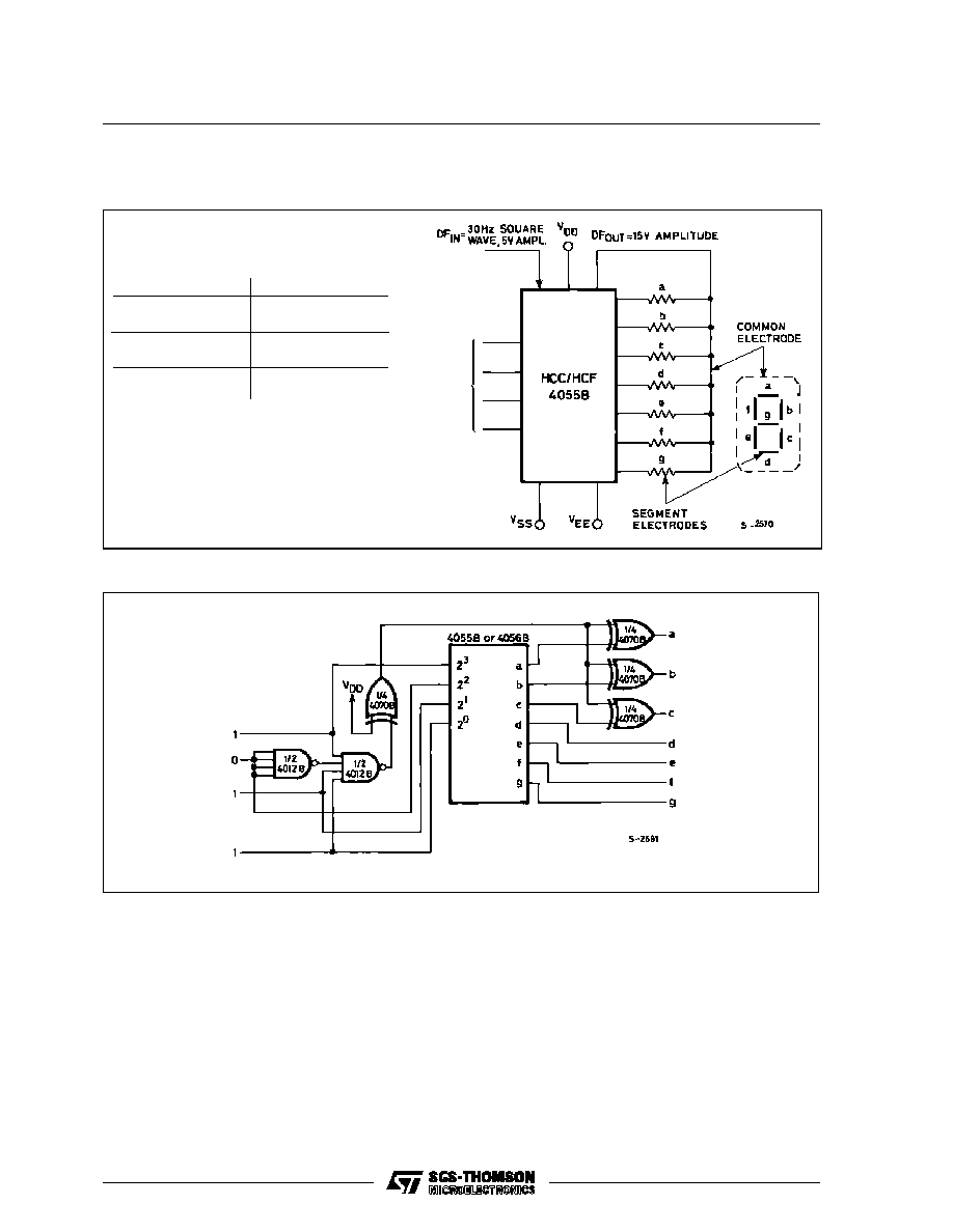
SS
should be at least 4V. The 7-seg-
ment outputs are controlled by the DISPLAY-FRE-
QUENCY (DF) input which causes the selected
segment outputs to be low, high, or a square-wave
output (for liquid-crystal displays). When the DF
input is low the output segments will be high when
selected by the BCD inputs. When the DF input is
high, the output segments will be low when selected
by the BCD inputs. When a square-wave is present
at the DF input, the selected segments will have a
square-wave output that is 180
∞
out of phase with
the DF input. Those segments which are not se-
lected will have a square-wave output that is in
phase with the input. DF square-wave repetition
rates for liquid-crystal displays usually range from
30Hz (well above flicker rate) to 200Hz (well below
the upper limit of the liquid-crystal frequency re-
sponse). The HCC/HCF4055B provides a level-
shifted high-amplitude DF output which is required
for driving the common electrode in liquid-crystal
displays. The HCC/HCF4056B provides a strobed-
latch function at the BCD inputs. Decoding of all
input combinations on the HCC/HCF4055B and
HCC/HCF4056B provides displays of 0 to 9 as well
1/15
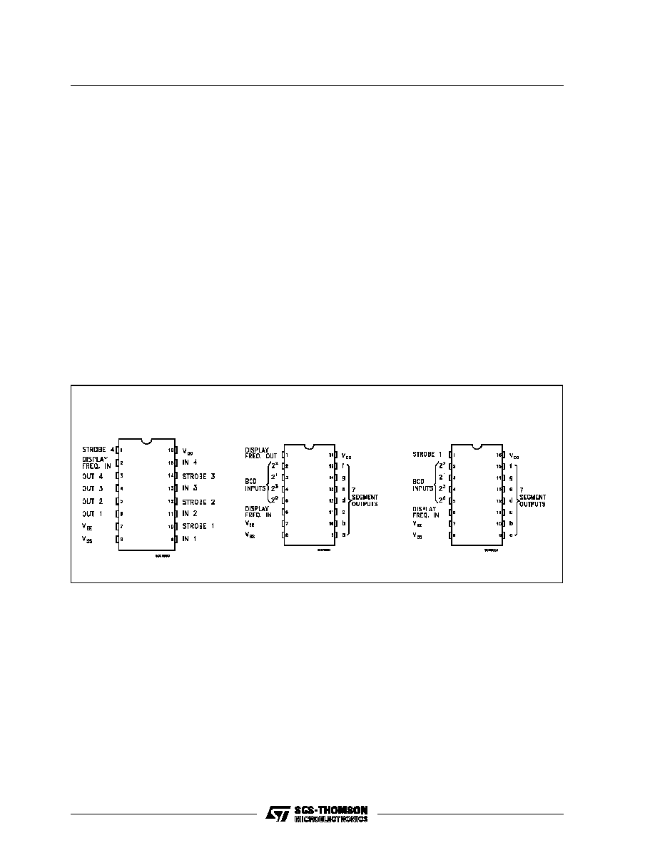
PIN CONNECTIONS
4054B
4055B
4056B
as L, P, H, A,≠ , and a blank position. (see typical ap-
plication for other letters). The HCC/HCF4054B pro-
vides level shifting similar to the HCC/HCF4055B
and HCC/HCF4056B independently strobed latches,
and common DF control on 4 signal lines. The
HCC/HCF4054B is intended to provide drive-signal
compatibility
with
the
HCC/HCF4055B
and
HCC/HCF4056B 7-segment decoder types for the
decimal point, colon, polarity, and similar display lines.
A level-shifted high-amplitude DF output can be ob-
tained from any HCC/HCF4054B output line by con-
necting the corresponding input and strobe lines to
a
low
and
high
level,
respectively.
The
HCC/HCF4054B may also be utilized for logic-level
"up conversion" or "down conversion". Forexample,
input-signal swings (V
DD
to V
SS
) from + 5 to 0V can
be converted to output-signal swings (V
DD
to V
EE
) of
+ 5 to ≠ 5V. The level-shifted function on all three
types permits the use of different input-and output-
signal swings. The input swings from a low level of
V
SS
to a high level of V
DD
while the output swings
from a low level of V
EE
to the same high level of V
DD
.
Thus, the input and output swings can be selected
independently of each other over a 3-to-18V range.
V
SS
may be connected to V
EE
when no level-shift
function is required. For the HCC/HCF 4054B and
HCC/HCF 4056B, data are transferred from input to
output by placing a high voltage level at the strobe
input. A low voltage level at the strobe input latches
the data input and the corresponding output seg-
ments remain selected (or non-selected) while the
strobe is low. Whenever the level-shifting function
is required, the HCC/HCF4055B can be used by it-
self to drive a liquid-crystal display (fig. 10 and fig.
12). The HCC/HCF4056B, however, must be used
together with a HCC/HCF4054B to provide the com-
mon DF output (fig. 14). The capability of extending
the voltage swing on the negative end (this voltage
cannot be extended on the positive end) can be
used to advantage in the set-up of fig. 11. Fig. 9 is
common to all three types.
HCC/HCF4054B/55B/56B
2/15
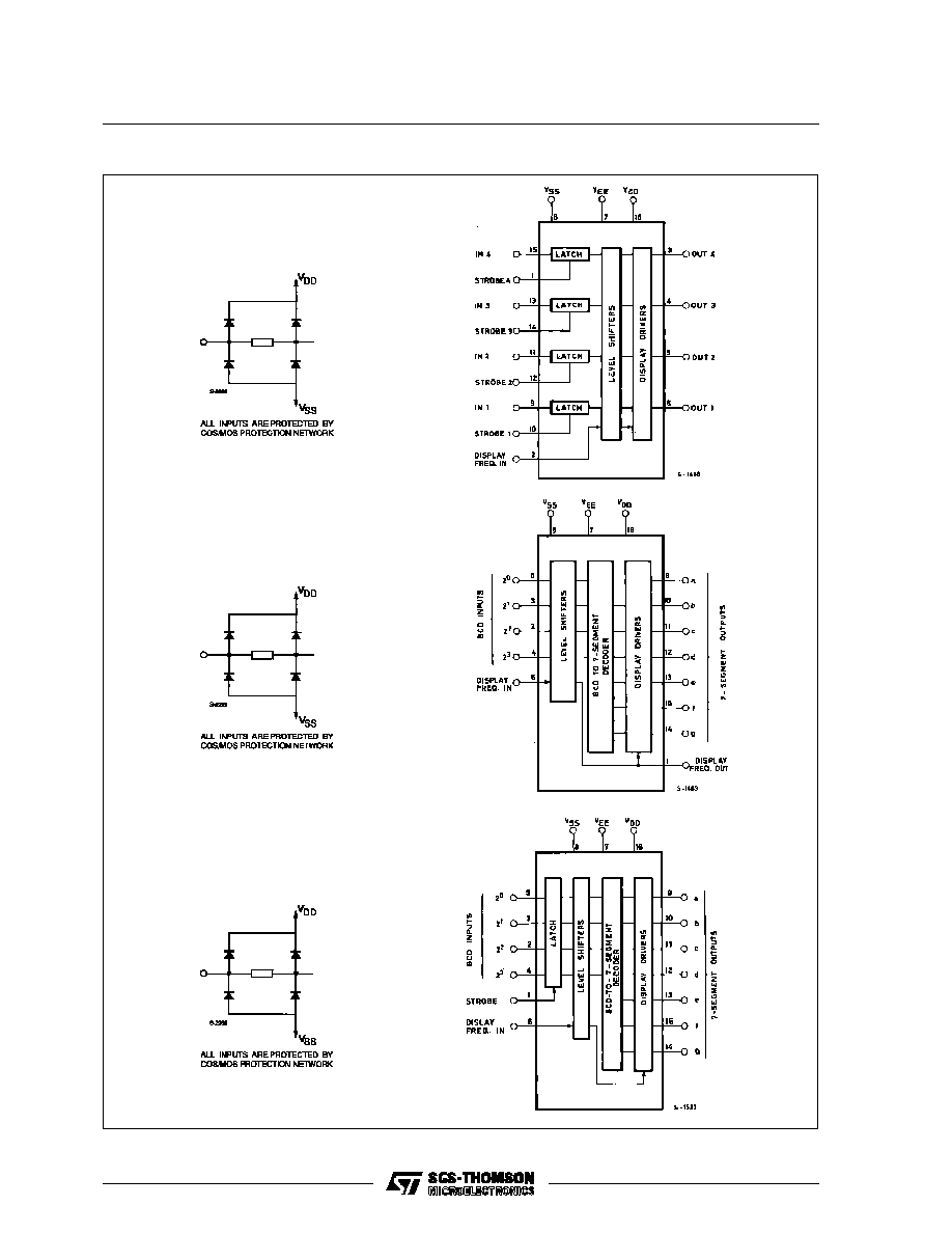
FUNCTIONAL DIAGRAMS
4054B
4055B
4056B
HCC/HCF4054B/55B/56B
3/15

ABSOLUTE MAXIMUM RATINGS
Symbol
Parameter
Value
Unit
V
DD
*
Supply Voltage : HC C Types
H C F Types
≠ 0.5 to + 20
≠ 0.5 to + 18
V
V
V
i
Input Voltage
≠ 0.5 to V
DD
+ 0.5
V
I
I
DC Input Current (any one input)
±
10
mA
P
t o t
Total Power Dissipation (per package)
Dissipation per Output Transistor
for T
o p
= Full Package-temperature Range
200
100
mW
mW
T
o p
Operating Temperature : HCC Types
H CF Types
≠ 55 to + 125
≠ 40 to + 85
∞
C
∞
C
T
s t g
Storage Temperature
≠ 65 to + 150
∞
C
RECOMMENDED OPERATING CONDITIONS
Symbol
Parameter
Val ue
Unit
V
DD
Supply Voltage : H CC Types
H C F Types
3 to 18
3 to 15
V
V
V
I
Input Voltage
0 to V
DD
V
T
o p
Operating Temperature : HCC Types
HC F Types
≠ 55 to 125
≠ 40 to 85
∞
C
∞
C
Stresses above those listed under "Absolute Maximum Ratings" may cause permanent damage to the device. This is a stress rating only
and functional operation of the device at these or any other conditions above those indicated in the operational sections of this specification
is not implied. Exposure to absolute maximum rating conditions for external periods may affect device reliability.
* All voltage values are referred to V
SS
pin voltage.
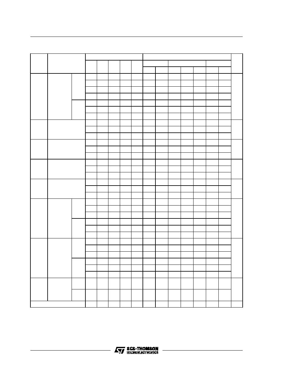
TRUTH TABLE
4055 B and 4056 B
Input Code
Output State
2
3
2
2
2
1
2
0
a
b
c
d
e
f
g
Display
Character
0
0
0
0
0
0
0
0
1
1
1
1
1
1
1
1
0
0
0
0
1
1
1
1
0
0
0
0
1
1
1
1
0
0
1
1
0
0
1
1
0
0
1
1
0
0
1
1
0
1
0
1
0
1
0
1
0
1
0
1
0
1
0
1
1
0
1
1
0
1
1
1
1
1
0
0
1
1
0
0
1
1
1
1
1
0
0
1
1
1
0
1
1
1
0
0
1
1
0
1
1
1
1
1
1
1
0
1
0
1
0
0
1
0
1
1
0
1
1
0
1
1
1
0
0
0
0
0
1
0
1
0
0
0
1
0
1
0
1
1
1
1
0
0
1
0
0
0
1
1
1
0
1
1
1
1
1
1
0
0
0
0
1
1
1
1
1
0
1
1
0
1
1
1
1
0
0
1
2
3
4
5
6
7
8
9
L
H
P
A
≠
BLANK
Data Setup Time and Strobe Pulse Duration.
HCC/HCF4054B/55B/56B
4/15
STATIC ELECTRICAL CHARACTERISTICS (over recommended operating conditions)
Test Conditions
Value
V
EE
V
I
V
O
V
SS
V
DD
T
Low
*
25
∞
C
T
Hi gh
*
Symbol
Parameter
(V)
(V)
(V)
(V)
(V)
Min.
Max.
Min.
Typ.
Max.
Min.
Max.
Unit
I
L
Quiescent
Supply
Current
HCC
Types
≠ 5
0/5
0
5
5
0.04
5
150
0
0/10
0
10
10
0.04
10
300
0
0/15
0
15
20
0.04
20
600
0
0/20
0
20
100
0.08
100
3000
HCF
Types
≠ 5
0/5
0
5
20
0.04
20
150
0
0/10
0
10
40
0.04
40
300
0
0/15
0
15
80
0.04
80
600
µ
A
V
OH
Output High
Voltage
0
0/5
0
5
4.95
4.95
4.95
V
0
0/10
0
10
9.95
9.95
9.95
0
0/15
0
15
14.95
14.95
14.95
V
OL
Output Low
Voltage
0
5/0
0
5
0.05
0.05
0.05
V
0
10/0
0
10
0.05
0.05
0.05
0
15/0
0
15
0.05
0.05
0.05
V
IH
Input High
Voltage
≠ 5
0.5/4.5
0
5
3.5
3.5
3.5
V
0
1/9
0
10
7
7
7
0
1.5/13.5
0
15
11
11
11
V
IL
Input Low
Voltage
5
0.5/4.5
0
5
1.5
1.5
1.5
V
0
9/1
0
10
3
3
3
0
1.5/13.5
0
15
4
4
4
I
OH
Output
High
Current
HCC
Types
≠ 5
0/5
4.5
0
5
≠ 0.6
≠ 0.45 ≠ 0.9
≠ 0.3
0
0/10
9.5
0
10
≠ 0.6
≠ 0.45 ≠ 0.9
≠ 0.3
0
0/15 13.5
0
15
≠ 1.9
≠ 1.5
≠ 3
≠ 1.1
HCF
Types
≠ 5
0/5
4.5
0
5
≠ 0.47
≠ 0.38 ≠ 0.9
≠ 0.28
0
0/10
9.5
0
10
≠ 0.47
≠ 0.38 ≠ 0.9
≠ 0.28
0
0/15 13.5
0
15
≠ 1.58
≠ 1.27
≠ 3
≠ 0.95
mA
I
OL
Output
Low
Current
HCC
Types
≠ 5
0/5
0.4
0
5
1.6
1.3
2.6
0.9
mA
0
0/10
0.5
0
10
1.6
1.3
2.6
0.9
0
0/15
1.5
0
15
4.2
3.4
6.8
2.4
HCF
Types
≠ 5
0/5
0.4
0
5
1.37
1.1
2.6
0.82
0
0/10
0.5
0
10
1.37
1.1
2.6
0.82
0
0/15
1.5
0
15
3.62
2.9
6.8
2.17
I
IH
, I
IL
**
Input
Leakage
Current
HCC
Types
0
0/18
0
18
±
0.1
±
10
≠5
±
0.1
±
1
HCF
Types
0
0/15
0
15
±
0.3
±
10
≠5
±
0.3
±
1
µ
A
µ
A
C
I
**
Input Capacitance
5
7.5
pF
* T
Low
= ≠ 55
∞
C for HCC device : ≠ 40
∞
C for HCF device.
* T
High
= 125
∞
C fr HCC device : + 85
∞
C for HCF device.
The Noise Margin for both "1" and "0" level is : 1V min. with V
DD
= 5V, 2V min. with V
DD
= 10V, 2.5 V min. with V
DD
= 15V.
** Any input.
HCC/HCF4054B/55B/56B
5/15
DYNAMIC ELECTRICAL CHARACTERISTICS (T
amb
= 25
∞
C, C
L
= 50pF, R
L
= 200k
,
typical temperature coefficient for all V
DD
values is 0.3%/
∞
C, all input rise and fall times = 20ns)
Test Conditions
Types
4054B
4055B, 4056B
Symbol
Parameter
V
E E
(V)
V
S S
(V)
V
D D
(V)
Mi n. Typ. Max. Min. Typ. Max.
Unit
t
PHL
, t
PL H
Propagation Delay Time (any
input to any output)
≠ 5
0
5
400
800
650 1300
ns
0
0
10
340
680
575 1150
0
0
15
250
500
375
750
t
T HL
, t
TL H
Transition Time (any output)
≠ 5
0
5
100
200
100
200
ns
0
0
10
100
200
100
200
0
0
15
75
150
75
150
t
se t u p
*
Data Setup Time
≠ 5
0
5
220
110
220
110
ns
0
0
10
100
50
100
50
0
0
15
70
35
70
35
t
W
*
Strobe Pulse Width
≠ 5
0
5
220
110
220
110
ns
0
0
10
100
50
100
50
0
0
15
70
35
70
35
* HCC/HCF4054B and HCC/HCF4056B only.
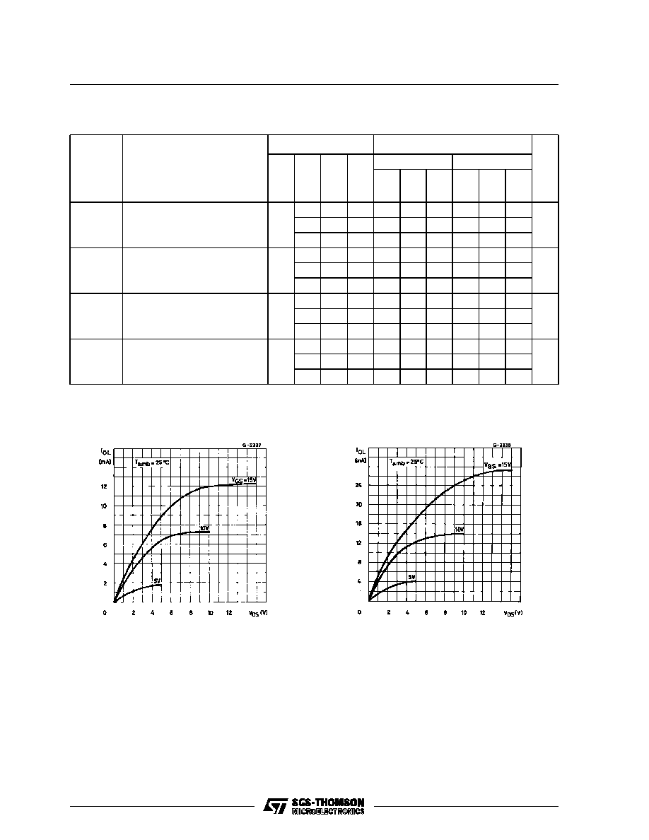
Figure 1 : Typical Output Low (sink) Current
Characteristics.
Figure 2 : Minimum Output High (source) Current
Characteristics.
HCC/HCF4054B/55B/56B
6/15

Figure 3 : Typical Output High (source) Current
Characteristics.
Figure 4 : Minimum Output (source) Current
Characteristics.
Figure 5 : Typical Propagation Delay Time vs.
Load Capacitance (for 4054B).
Figure 6 : Typical Propagation Delay Time vs. Load
Capacitance (for 4055B and 4056B).
Figure 7 : Typical Transition Time vs. Load Capa-
citance.
Figure 8 : Typical Dynamic Power Dissipation vs.
Frequency.
HCC/HCF4054B/55B/56B
7/15

TYPICAL APPLICATIONS
Figure 9 : Display-driver Circuit for one Segment Line and Waveforms.
(a)
(b)
Figure 10 : Clock Display.
Figure 11 : Digital (0 to + 5V) to bidirectional Analog
Control (+ 5 to ≠ 5V) Level Shifter.
V
DD
= 0V, V
SS
= ≠ 5V, V
EE
= ≠ 15V, F
IN
= 30 Hz square wave.
HCC/HCF4054B/55B/56B
8/15
TYPICAL APLLICATIONS (continued)
Figure 12 : Single-digit Liquid Crystal Display.
BCD IN FROM
DTL, TTL, OR
COS/MOS LOGIC
OPTION 1
V
DD
0V
V
SS
≠5V
V
EE
≠15V
OPTION 2
V
DD
+ 5V
V
SS
0V
V
EE
≠ 10V
Figure 13 : Conversion of "H" Display to "F" Display.
HCC/HCF4054B/55B/56B
9/15
TYPICAL APLLICATIONS (continued)
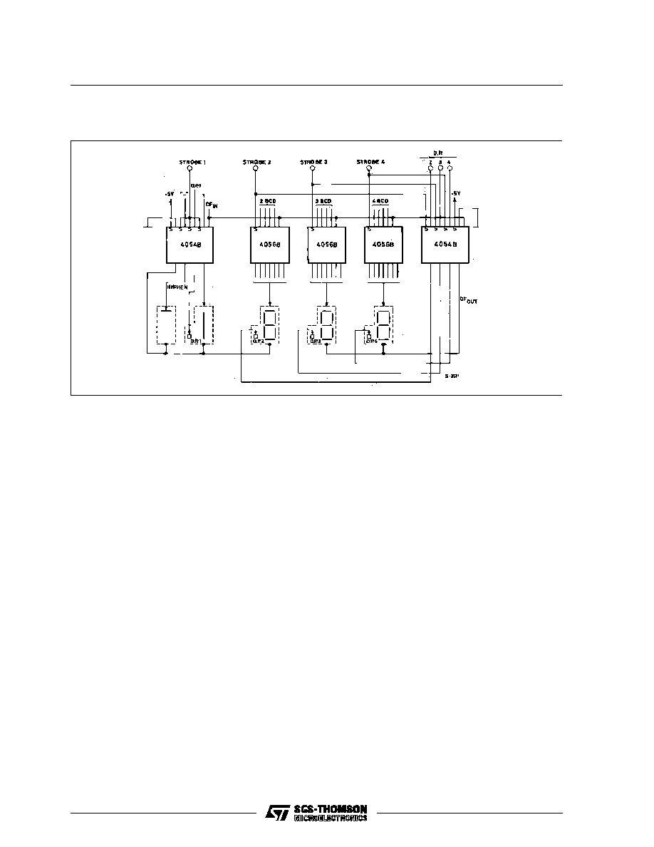
Figure 14 : Typical 3
1
/
2
≠ Digit≠crystal Display : (V
DD
= + 5V, V
SS
= 0V, V
EE
= ≠ 10V, DF
N
= 30 Hz square).
In addition to the letters L, H, P, and A, five other let-
ters can be displayed through the use of simple
logic
circuits
preceding
and
following
the
HCC/HCF4055B or
HCC/HCF4056B
devices.
Fig. 13 is an example of a circuit that converts an "H"
display, (code 1011) to an "F" display. One condition
that must be met is that V
EE
= V
SS
. If V
EE
V
SS
, the
HCC/HCF4054B must be used to level shift in the
appropriate places. In a similar manner the letters C,
E, J,and U can be displayed. These circuits can also
be used to drive LED displays provided the exclu-
sive-OR gates have sufficient output-current drive.
The letters B, D, G, I, O, and S may be represented
by the codes for numbers 8, 0, 6, 1, 0, and 5, respec-
tively, when there is preknowledge that only letters
are to be displayed.
HCC/HCF4054B/55B/56B
10/15
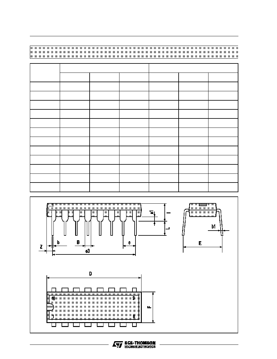
Plastic DIP16 (0.25) MECHANICAL DATA
DIM.
mm
inch
MIN.
TYP.
MAX.
MIN.
TYP.
MAX.
a1
0.51
0.020
B
0.77
1.65
0.030
0.065
b
0.5
0.020
b1
0.25
0.010
D
20
0.787
E
8.5
0.335
e
2.54
0.100
e3
17.78
0.700
F
7.1
0.280
I
5.1
0.201
L
3.3
0.130
Z
1.27
0.050
P001C
HCC/HCF4054B/55B/56B
11/15

Ceramic DIP16/1 MECHANICAL DATA
DIM.
mm
inch
MIN.
TYP.
MAX.
MIN.
TYP.
MAX.
A
20
0.787
B
7
0.276
D
3.3
0.130
E
0.38
0.015
e3
17.78
0.700
F
2.29
2.79
0.090
0.110
G
0.4
0.55
0.016
0.022
H
1.17
1.52
0.046
0.060
L
0.22
0.31
0.009
0.012
M
0.51
1.27
0.020
0.050
N
10.3
0.406
P
7.8
8.05
0.307
0.317
Q
5.08
0.200
P053D
HCC/HCF4054B/55B/56B
12/15
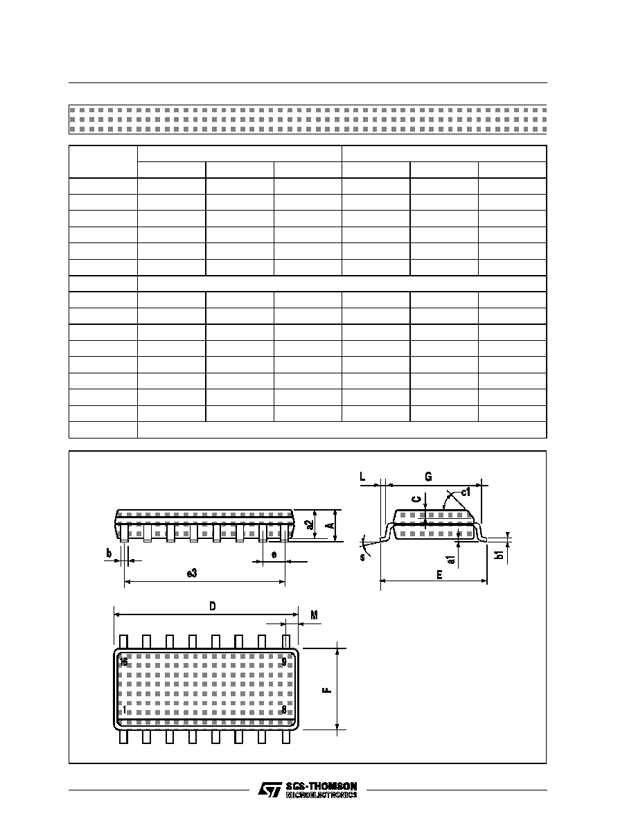
SO16 (Narrow) MECHANICAL DATA
DIM.
mm
inch
MIN.
TYP.
MAX.
MIN.
TYP.
MAX.
A
1.75
0.068
a1
0.1
0.2
0.004
0.007
a2
1.65
0.064
b
0.35
0.46
0.013
0.018
b1
0.19
0.25
0.007
0.010
C
0.5
0.019
c1
45
∞
(typ.)
D
9.8
10
0.385
0.393
E
5.8
6.2
0.228
0.244
e
1.27
0.050
e3
8.89
0.350
F
3.8
4.0
0.149
0.157
G
4.6
5.3
0.181
0.208
L
0.5
1.27
0.019
0.050
M
0.62
0.024
S
8
∞
(max.)
P013H
HCC/HCF4054B/55B/56B
13/15

PLCC20 MECHANICAL DATA
DIM.
mm
inch
MIN.
TYP.
MAX.
MIN.
TYP.
MAX.
A
9.78
10.03
0.385
0.395
B
8.89
9.04
0.350
0.356
D
4.2
4.57
0.165
0.180
d1
2.54
0.100
d2
0.56
0.022
E
7.37
8.38
0.290
0.330
e
1.27
0.050
e3
5.08
0.200
F
0.38
0.015
G
0.101
0.004
M
1.27
0.050
M1
1.14
0.045
P027A
HCC/HCF4054B/55B/56B
14/15

Information furnished is believed to be accurate and reliable. However, SGS-THOMSON Microelectronics assumes no responsability for the
consequences of use of such information nor for any infringement of patents or other rights of third parties which may results from its use. No
license is granted by implication or otherwise under any patent or patent rights of SGS-THOMSON Microelectronics. Specifications mentioned
in this publication are subject to change without notice. This publication supersedes and replaces all information previously supplied.
SGS-THOMSON Microelectronics products are not authorized for use as critical components in life support devices or systems without express
written approval of SGS-THOMSON Microelectonics.
©
1994 SGS-THOMSON Microelectronics - All Rights Reserved
SGS-THOMSON Microelectronics GROUP OF COMPANIES
Australia - Brazil - France - Germany - Hong Kong - Italy - Japan - Korea - Malaysia - Malta - Morocco - The Netherlands -
Singapore - Spain - Sweden - Switzerland - Taiwan - Thailand - United Kingdom - U.S.A
HCC/HCF4054B/55B/56B
15/15