 | –≠–ª–µ–∫—Ç—Ä–æ–Ω–Ω—ã–π –∫–æ–º–ø–æ–Ω–µ–Ω—Ç: HCC4060 | –°–∫–∞—á–∞—Ç—å:  PDF PDF  ZIP ZIP |

HCC4060B
HCF4060B
September 1988
COUNTER/DIVIDER AND OSCILLATOR
14-STAGE RIPPLE CARRY BINARY
EY
(Plastic Package)
DESCRIPTION
ORDER CODES :
HCC4060BF
HCF4060BM1
HCF4060BEY
HCF4060BC1
F
(Ceramic Package)
M1
(Micro Package)
C1
(Chip Carrier)
PIN CONNECTIONS
.
MEDIUM-SPEED OPERATION
.
COMMON RESET
.
FULLY STATIC OPERATION
.
BUFFERED INPUTS AND OUTPUTS
.
QUIESCENT CURRENT SPECIFIED TO 20V
FOR HCC DEVICE
.
5V, 10V AND 15V PARAMETRIC RATINGS
.
INPUT CURRENT OF 100nA AT 18V AND 25
o
C
FOR HCC DEVICE
.
1005 TESTED FOR QUIESCENT CURRENT
.
MEETS ALL REQUIREMENTS OF JEDEC TEN-
TATIVE STANDARD N. 13A, " STANDARD
SPECIFICATIONS FOR DESCRIPTION OF ' B
' SERIES CMOS DEVICES "
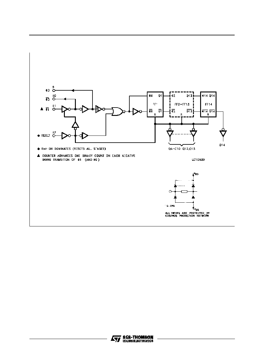
The HCC4060B (extended temperature range) and
HCF4060B (intermediate temperature range) are
monolithic integrated circuit, available in 16-lead
dual in line plastic or ceramic package and plastic
micropackage. The HCC/HCF4060B consist of an
oscillator section and 14 ripple carry binary counter
stages. The oscillator configuration allows design of
either RC or crystal oscillator circuits. A RESET
input is provided which reset the counter to the all
0's state and disables oscillator. A high level on the
RESET line accmplishes the reset function. All
counter stages are master slave flip-flops. The state
of the counter is advanced one step in binary order
on the negative transition of
1
(and
0
). All inputs
and outputs are fully buffered. Schmitt trigger action
on the clock lin permits unlimited clock rise and fall
time.
1/13

FUNCTIONAL DIAGRAM
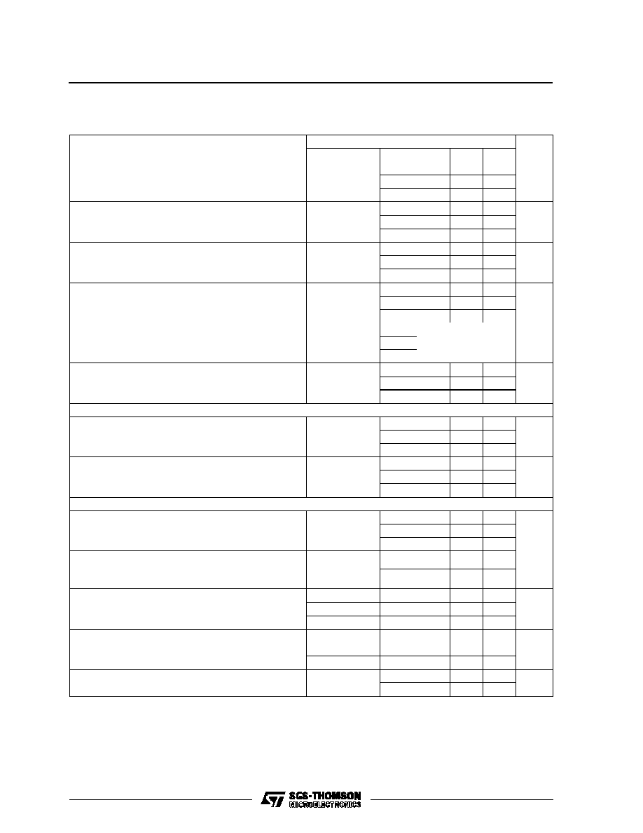
ABSOLUTE MAXIMUM RATING
Symbol
Parameter
Value
Unit
V
DD
*
Supply Voltage: HCC Types
HCF Types
-0.5 to +20
-0.5 to +18
V
V
V
i
Input Voltage
-0.5 to V
DD
+ 0.5
V
I
I
DC Input Current (any one input)
±
10
mA
P
tot
Total Power Dissipation (per package)
Dissipation per Output Transistor
for Top = Full Package Temperature Range
200
100
mW
mW
T
op
Operating Temperature: HCC Types
HCF Types
-55 to +125
-40 to +85
o
C
o
C
T
stg
Storage Temperature
-65 to +150
o
C
Stresses above those listed under "Absolute Maximum Ratings" may cause permanent damage to the device. This is a stress ratingonly and functional
operation of the device at these or any other conditions above those indicated in the operational sections of this specification is not implied. Exposure
to absolute maximum rating conditions for external periods may affect device reliability.
* All voltage values are referred to V
SS
pin voltage.
RECOMMENDED OPERATING CONDITIONS
Symbol
Parameter
Value
Unit
V
DD
Supply Voltage: HCC Types
HCF Types
3 to 18
3 to 15
V
V
V
I
Input Voltage
0 to V
DD
V
T
op
Operating Temperature: HCC Types
HCF Types
-55 to +125
-40 to +85
o
C
o
C
HCC/HCF4060B
2/13
LOGIC DIAGRAM
HCC/HCF4060B
3/13

STATIC ELECTRICAL CHARACTERISTICS (over recommended operating conditions)
Symbol
Parameter
Test Conditios
Value
Unit
V
I
(V)
V
O
(V)
|I
O
|
(
µ
A)
V
DD
(V)
T
LOW
*
25
o
C
T
HIGH
*
Min.
Max.
Min.
Typ.
Max.
Min.
Max.
I
L
Quiescent
Current
HCC
Types
0/5
5
5
0.04
5
150
µ
A
0/10
10
10
0.04
10
300
0/15
15
20
0.04
20
600
0/20
20
100
0.08
100
3000
HCF
Types
0/5
5
20
0.04
20
150
0/10
10
40
0.04
40
300
0/15
15
80
0.04
80
600
V
OH
Output High
Voltage
0/5
< 1
5
4.95
4.95
4.95
V
0/10
< 1
10
9.95
9.95
9.95
0/15
< 1
15
14.95
14.95
14.95
V
OL
Output Low
Voltage
5/0
< 1
5
0.05
0.05
0.05
V
10/0
< 1
10
0.05
0.05
0.05
15/0
< 1
15
0.05
0.05
0.05
V
IH
Input High
Voltage
0.5/4.5
< 1
5
3.5
3.5
3.5
V
1/9
< 1
10
7
7
7
1.5/13.5
< 1
15
11
11
11
V
IL
Input Low
Voltage
4.5/0.5
< 1
5
1.5
1.5
1.5
V
9/1
< 1
10
3
3
3
13.5/1.5
< 1
15
4
4
4
I
OH
Output
Drive
Current
HCC
Types
0/5
2.5
5
-2
-1.6
-3.2
-1.15
mA
0/5
4.6
5
-0.64
-0.51
-1
-0.36
0/10
9.5
10
-1.6
-1.3
-2.6
-0.9
0/15
13.5
15
-4.2
-3.4
-6.8
-2.4
HCF
Types
0/5
2.5
5
-1.53
-1.36
-3.2
-1.1
0/5
4.6
5
-0.52
-0.44
-1
-0.36
0/10
9.5
10
-1.3
-1.1
-2.6
-0.9
0/15
13.5
15
-3.6
-3.0
-6.8
-2.4
I
OL
Output
Sink
Current
HCC
Types
0/5
0.4
5
0.64
0.51
1
0.36
mA
0/10
0.5
10
1.6
1.3
2.6
0.9
0/15
1.5
15
4.2
3.4
6.8
2.4
HCF
Types
0/5
0.4
5
0.52
0.44
1
0.36
0/10
0.5
10
1.3
1.1
2.6
0.9
0/15
1.5
15
3.6
3.0
6.8
2.4
I
IH
, I
IL
Input Leakage
Current
0/18
Any Input
18
±
0.1
±
10
-5
±
0.1
±
1
µ
A
0/15
15
±
0.3
±
10
-5
±
0.3
±
1
µ
A
C
I
Input Capacitance
Any Input
5
7.5
pF
* T
LOW
= -55
o
C for HCC device: -40
o
C for HCF device.
* T
HIGH
= +125
o
C for HCC device: +85
o
C for HCF device.
The Noise Margin for both "1" and "0" level is: 1V min. with V
DD
= 5 V, 2 V min. with V
DD
= 10 V, 2.5 V min. with V
DD
= 15 V
HCC/HCF4060B
4/13
DYNAMIC ELECTRICAL CHARACTERISTICS (T
amb
= 25
o
C, C
L
= 50 pF, R
L
= 200 K
,
typical temperature coefficent for all V
DD
values is 03 %/
o
C, all input rise and fall times= 20 ns)
Symbol
Parameter
Test Conditions
Value
Unit
V
DD
(V)
Min.
Typ.
Max.
t
PLH
t
PHL
Propagation Delay Time
(
to Q4 out)
5
370
740
ns
10
150
300
15
100
200
t
PLH
t
PHL
Propagation Delay Time
(Qn to Q
n+1
)
5
100
200
ns
10
50
100
15
40
80
t
TLH
t
THL
Transition Time
5
100
200
ns
10
50
100
15
40
80
t
W
Input Pulse Width
f = 100KHz
5
50
100
ns
10
20
40
15
15
30
t
r
, t
f
Input Pulse Rise and Fall Time
5
Unlimited
µ
s
10
15
f
max
Maximum Clock Input Frequency
5
3.5
7
MHz
10
8
16
15
12
24
RESET OPERATION
t
PHL
Propagation Delay Time
5
180
360
ns
10
80
160
15
50
100
t
W
Reset Pulse Width
5
60
120
ns
10
30
60
15
20
40
RC OPERATION
Variation of Frequency (Unit-to-Unit)
C
X
= 200pF
R
S
= 560K
R
X
= 50 K
5
18
21.5
25
KHz
10
20
23
26
15
21.1
24
27
Variation of Frequency With Voltage Change
(Same Unit)
C
X
= 200pF
R
S
= 560K
R
X
= 50 K
5 to 10
2
10 to 15
1
R
X
C
X
= 10
µ
F
5
20
M
C
X
= 50
µ
F
10
20
C
X
= 10
µ
F
15
10
C
X
R
X
= 500 K
5
1000
mF
R
X
= 300 K
10
50
R
X
= 300 K
15
50
Maximum Oscillator Frequency *
R
X
= 5K
C
X
= 15pF
10
530
650
810
pF
15
690
800
94
* RC oscillator applications are not recommended at supply voltages below 7V for R
X
= 50K
HCC/HCF4060B
5/13