 | –≠–ª–µ–∫—Ç—Ä–æ–Ω–Ω—ã–π –∫–æ–º–ø–æ–Ω–µ–Ω—Ç: HCC4076BF | –°–∫–∞—á–∞—Ç—å:  PDF PDF  ZIP ZIP |
HCC4076B
HCF4076B
September 1988
4 BIT D TYPE REGISTERS
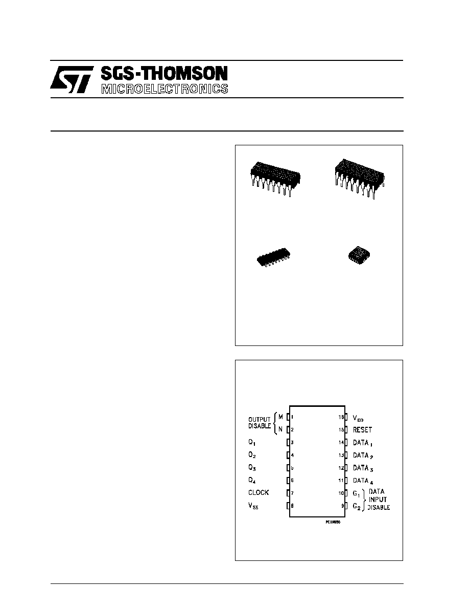
EY
(Plastic Package)
DESCRIPTION
ORDER CODES :
HCC4076BF
HCF4076BM1
HCF4076BEY
HCF4076BC1
F
(Ceramic Package)
M1
(Micro Package)
C1
(Chip Carrier)
PIN CONNECTIONS
The HCC4076B (extended temperature range) and
HCC4076B (intermediate temperature range) are
monolithic integrated circuit, available in 16 lead
dual in line plastic or ceramic package and plastic
micropackage.
The HCC/HCF4076B types are four-bit registers
consisting of D-type flip-flops that feature three-
state outputs. Data Disable inputs are provided to
control the entry of data into theflip-flops. When both
Data Disable inputs are low, data at the D inputs are
loaded into their respective flip-flops on the next
positive transition of the click input. Output Disable
inputs are also provided. When the Output Disable
inputs are both low, the normal logic states of the
four outputs are available to the load. The outputs
are disabled independently of the clock by a high
logic level at either Output Disable input, and pres-
ent a high impedance.
.
THREE STATE OUTPUTS
.
INPUT DISABLE WITHOUT GATING THE
CLOCK
.
GATED OUTPUT CONTROL LINES FOR EN-
ABLING OR DISABLING THE OUTPUTS
.
QUIESCENT CURRENT SPECIFIED TO 20V
FOR HCC DEVICE
.
5V, 10V AND 15V PARAMETRIC RATINGS
.
INPUT CURRENT OF 100nA AT 18V AND 25
o
C
FOR HCC DEVICE
.
100% TESTED FOR QUIESCENT CURRENT
.
MEETS ALL REQUIREMENTS OF JEDEC TEN-
TATIVE STANDARD N. 13A, " STANDARD
SPECIFICATIONS FOR DESCRIPTION OF B
SERIES CMOS DEVICES "
1/13
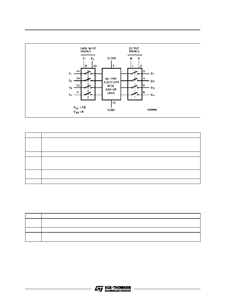
FUNCTIONAL DIAGRAM
ABSOLUTE MAXIMUM RATING
Symbol
Parameter
Value
Unit
V
DD
*
Supply Voltage: HCC Types
HCF Types
-0.5 to +20
-0.5 to +18
V
V
V
i
Input Voltage
-0.5 to V
DD
+ 0.5
V
I
I
DC Input Current (any one input)
±
10
mA
P
tot
Total Power Dissipation (per package)
Dissipation per Output Transistor
for Top = Full Package Temperature Range
200
100
mW
mW
T
op
Operating Temperature: HCC Types
HCF Types
-55 to +125
-40 to +85
o
C
o
C
T
stg
Storage Temperature
-65 to +150
o
C
Stresses above those listed under "Absolute Maximum Ratings" may cause permanent damage to the device. This is a stress ratingonly and functional
operation of the device at these or any other conditions above those indicated in the operational sections of this specification is not implied. Exposure
to absolute maximum rating conditions for external periods may affect device reliability.
* All voltage values are referred to V
SS
pin voltage.
RECOMMENDED OPERATING CONDITIONS
Symbol
Parameter
Value
Unit
V
DD
Supply Voltage: HCC Types
HCF Types
3 to 18
3 to 15
V
V
V
I
Input Voltage
0 to V
DD
V
T
op
Operating Temperature: HCC Types
HCF Types
-55 to +125
-40 to +85
o
C
o
C
HCC/HCF4076B
2/13
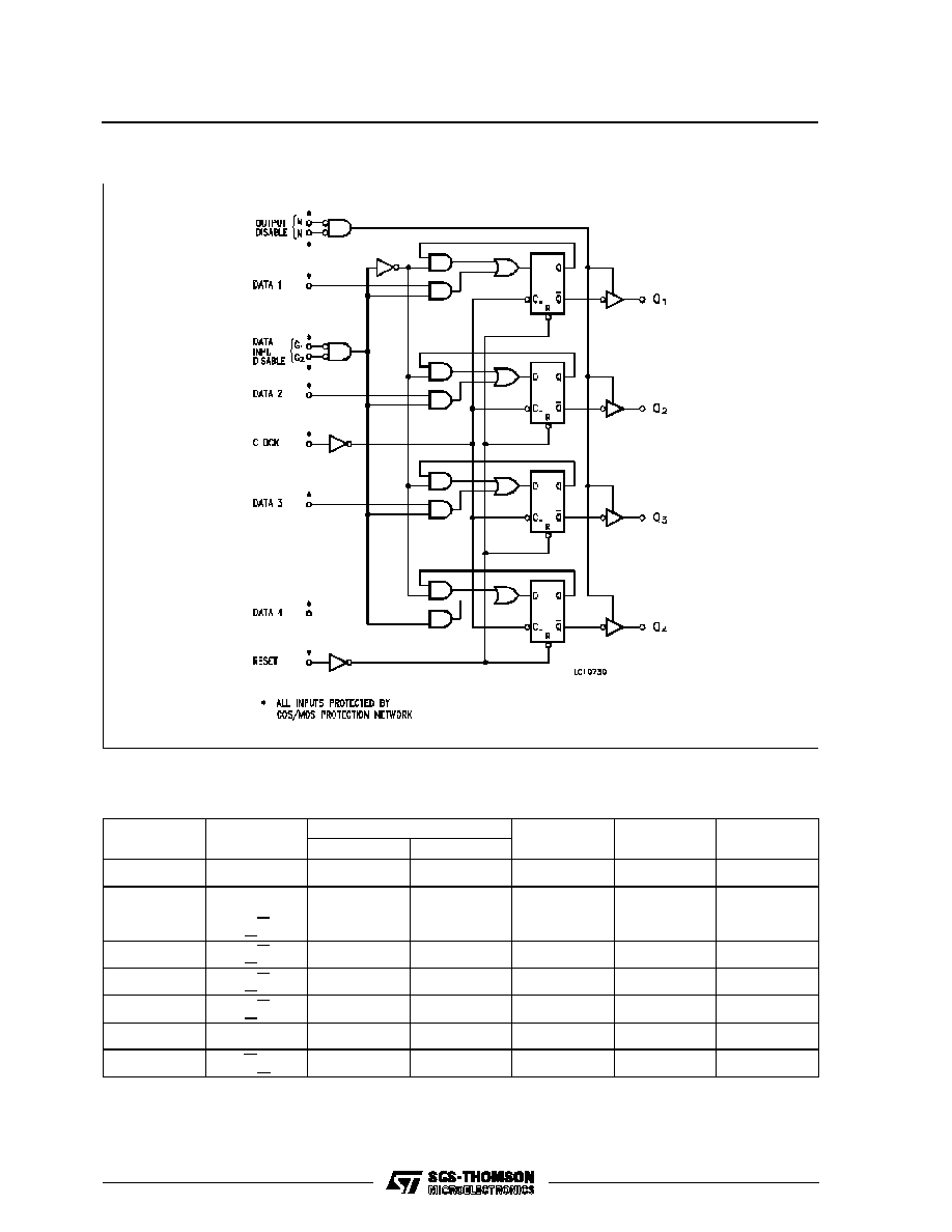
LOGIC DIAGRAM
TRUTH TABLE
RESET
CLOCK
DATA INPUT DISABLE
DATA
D
NEXT STATE
OUTPUT G
G1
G2
1
X
X
X
X
0
0
0
X
X
X
Q
NC
0
1
X
X
Q
NC
0
X
1
X
Q
NC
0
0
0
1
1
0
0
0
0
0
0
1
X
X
X
Q
NC
0
X
X
X
Q
NC
When either Output DisableM or N is high, theoutputs aredisablesd (high impedance state): however sequential operation of the flip-flopis not affected.
1 = High Level, 0 = Low Level, X = Don't Care, NC = No Change
HCC/HCF4076B
3/13
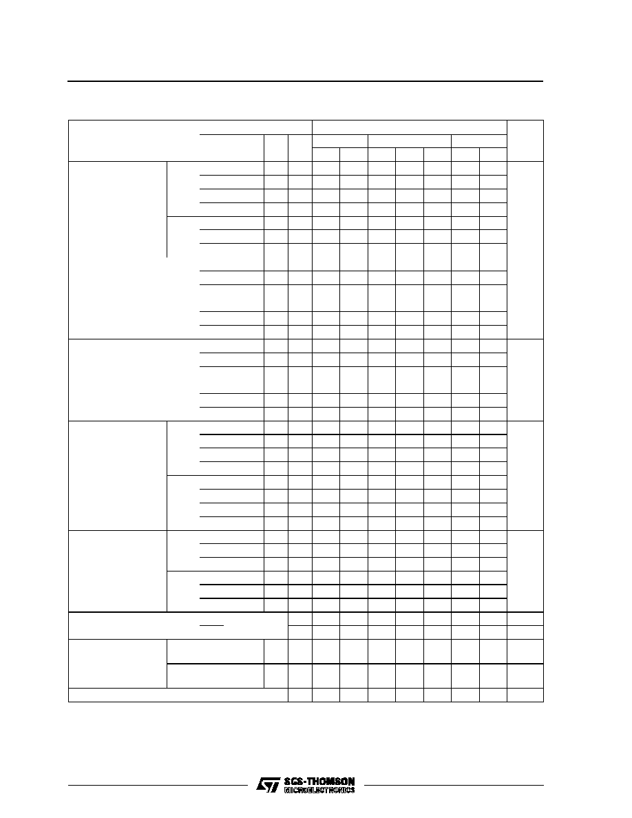
STATIC ELECTRICAL CHARACTERISTICS (over recommended operating conditions)
Symbol
Parameter
Test Conditios
Value
Unit
V
I
(V)
V
O
(V)
|I
O
|
(
µ
A)
V
DD
(V)
T
LOW
*
25
o
C
T
HIGH
*
Min.
Max.
Min.
Typ.
Max.
Min.
Max.
I
L
Quiescent
Current
HCC
Types
0/5
5
5
0.04
5
150
µ
A
0/10
10
10
0.04
10
300
0/15
15
20
0.04
20
600
0/20
20
100
0.08
100
3000
HCF
Types
0/5
5
20
0.04
20
150
0/10
10
40
0.04
40
300
0/15
15
80
0.04
80
600
V
OH
Output High
Voltage
0/5
< 1
5
4.95
4.95
4.95
V
0/10
< 1
10
9.95
9.95
9.95
0/15
< 1
15
14.95
14.95
14.95
V
OL
Output Low
Voltage
5/0
< 1
5
0.05
0.05
0.05
V
10/0
< 1
10
0.05
0.05
0.05
15/0
< 1
15
0.05
0.05
0.05
V
IH
Input High
Voltage
0.5/4.5
< 1
5
3.5
3.5
3.5
V
1/9
< 1
10
7
7
7
1.5/13.5
< 1
15
11
11
11
V
IL
Input Low
Voltage
4.5/0.5
< 1
5
1.5
1.5
1.5
V
9/1
< 1
10
3
3
3
13.5/1.5
< 1
15
4
4
4
I
OH
Output
Drive
Current
HCC
Types
0/5
2.5
5
-2
-1.6
-3.2
-1.15
mA
0/5
4.6
5
-0.64
-0.51
-1
-0.36
0/10
9.5
10
-1.6
-1.3
-2.6
-0.9
0/15
13.5
15
-4.2
-3.4
-6.8
-2.4
HCF
Types
0/5
2.5
5
-1.53
-1.36
-3.2
-1.1
0/5
4.6
5
-0.52
-0.44
-1
-0.36
0/10
9.5
10
-1.3
-1.1
-2.6
-0.9
0/15
13.5
15
-3.6
-3.0
-6.8
-2.4
I
OL
Output
Sink
Current
HCC
Types
0/5
0.4
5
0.64
0.51
1
0.36
mA
0/10
0.5
10
1.6
1.3
2.6
0.9
0/15
1.5
15
4.2
3.4
6.8
2.4
HCF
Types
0/5
0.4
5
0.61
0.44
1
0.36
0/10
0.5
10
1.
1.1
2.6
0.9
0/15
1.5
15
3.6
3.0
6.8
2.4
I
IH
, I
IL
Input Leakage
Current
0/18
Any Input
18
±
0.1
±
10
-5
±
0.1
±
1
µ
A
0/15
15
±
0.3
±
10
-5
±
0.3
±
1
µ
A
I
OH
, I
OL
Input
Leakage
Current
HCC
Types
0/18
0/18
18
±
0.4
±
10
-4
±
0.4
±
12
µ
A
HCF
Types
0/15
0/15
15
±
1.0
±
10
-4
±
1.0
±
7.5
µ
A
C
I
Input Capacitance
Any Input
5
7.5
pF
* T
LOW
= -55
o
C for HCC device: -40
o
C for HCF device.
* T
HIGH
= +125
o
C for HCC device: +85
o
C for HCF device.
The Noise Margin for both "1" and "0" level is: 1V min. with V
DD
= 5 V, 2 V min. with V
DD
= 10 V, 2.5 V min. with V
DD
= 15 V
HCC/HCF4076B
4/13
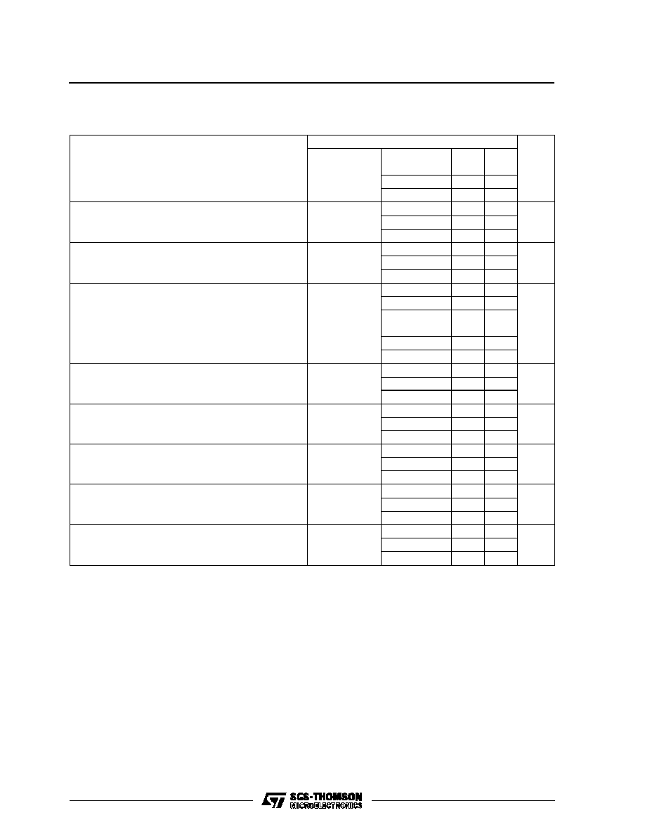
DYNAMIC ELECTRICAL CHARACTERISTICS (T
amb
= 25
o
C, C
L
= 50 pF, R
L
= 200 K
,
typical temperature coefficent for all V
DD
values is 03 %/
o
C, all input rise and fall times= 20 ns)
Symbol
Parameter
Test Conditions
Value
Unit
V
DD
(V)
Min.
Typ.
Max.
t
PLH
t
PHL
Propagation Delay Time
(Clock to Q Output)
5
300
600
ns
10
125
250
15
90
180
t
PHL
(R)
Propagation Delay Time
(Reset)
5
230
460
ns
10
100
200
15
75
150
t
P(1-H)
t
P(0-H)
3-State Output 1 or 0 to High Impedance
R
L
= 1K
5
150
300
ns
10
75
150
15
60
120
t
P(H-1)
t
P(L-1)
3-State High Impedance to 1 or 0 Output
R
L
= 1K
5
150
300
ns
10
75
150
15
60
120
t
W
Clock Pulse Width
5
200
100
ns
10
100
50
15
80
40
t
W
Reset Pulse Width
5
120
60
ns
10
50
25
15
40
20
t
setup
Data Setup Time
5
200
100
ns
10
80
40
15
60
30
t
setup
Data Input Disable Setup Time
5
180
90
ns
10
100
50
15
70
35
f
max
Maximum Clock Frequency
5
3
6
MHz
10
6
12
15
8
16
t
r
, t
f
Clock Input Rise or Fall Time
5
15
µ
s
10
5
15
5
HCC/HCF4076B
5/13
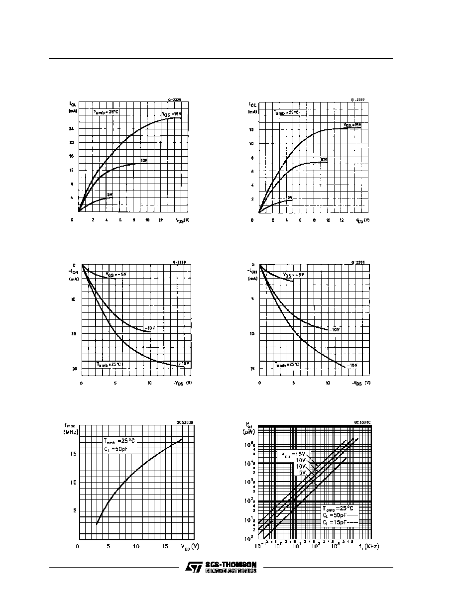
Typical Output Low (sink) Current Characteristics
Typical Output High (source) Current Charac-
teristics
Typical Maximum Clock Input Frequency vs Sup-
ply Voltage
Minimum Output Low (sink) Current Charac-
teristics
Minimum Output High (source) Current Charac-
teristics
Typical Dynamic Power Dissipation vs Fre-
quency
HCC/HCF4076B
6/13
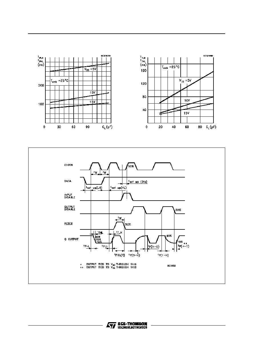
Typical Propagation Delay Time vs Capacitance
WAVEFORMS
Typical Transition Time vs Load Capacitance
HCC/HCF4076B
7/13
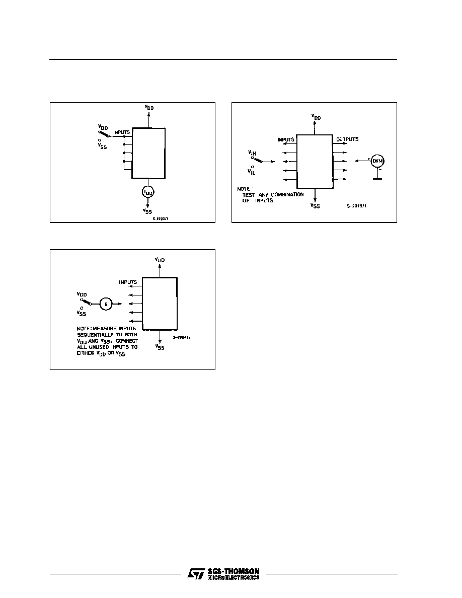
Quiescent Device Current.
Noise Immunity.
Input Leakage Current.
TEST CIRCUITS
HCC/HCF4076B
8/13
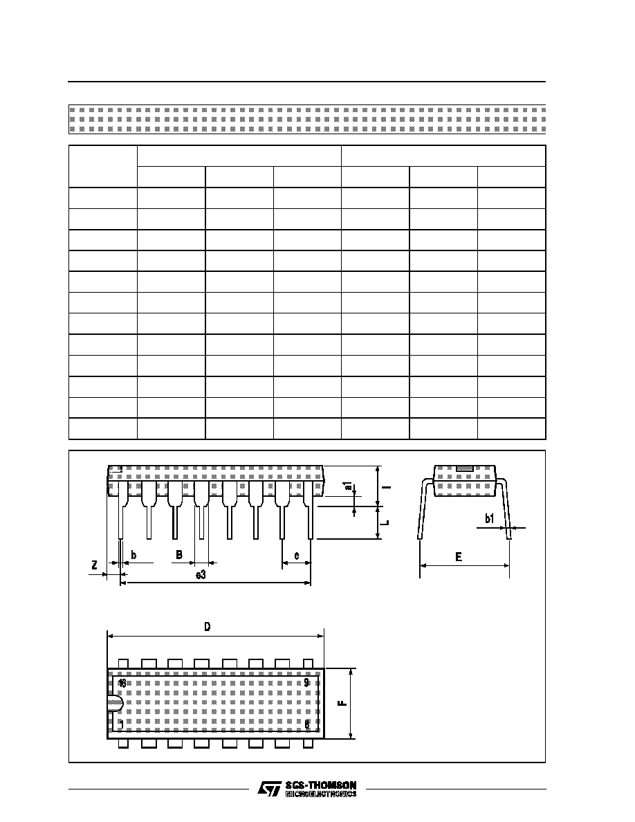
Plastic DIP16 (0.25) MECHANICAL DATA
DIM.
mm
inch
MIN.
TYP.
MAX.
MIN.
TYP.
MAX.
a1
0.51
0.020
B
0.77
1.65
0.030
0.065
b
0.5
0.020
b1
0.25
0.010
D
20
0.787
E
8.5
0.335
e
2.54
0.100
e3
17.78
0.700
F
7.1
0.280
I
5.1
0.201
L
3.3
0.130
Z
1.27
0.050
P001C
HCC/HCF4076B
9/13

Ceramic DIP16/1 MECHANICAL DATA
DIM.
mm
inch
MIN.
TYP.
MAX.
MIN.
TYP.
MAX.
A
20
0.787
B
7
0.276
D
3.3
0.130
E
0.38
0.015
e3
17.78
0.700
F
2.29
2.79
0.090
0.110
G
0.4
0.55
0.016
0.022
H
1.17
1.52
0.046
0.060
L
0.22
0.31
0.009
0.012
M
0.51
1.27
0.020
0.050
N
10.3
0.406
P
7.8
8.05
0.307
0.317
Q
5.08
0.200
P053D
HCC/HCF4076B
10/13
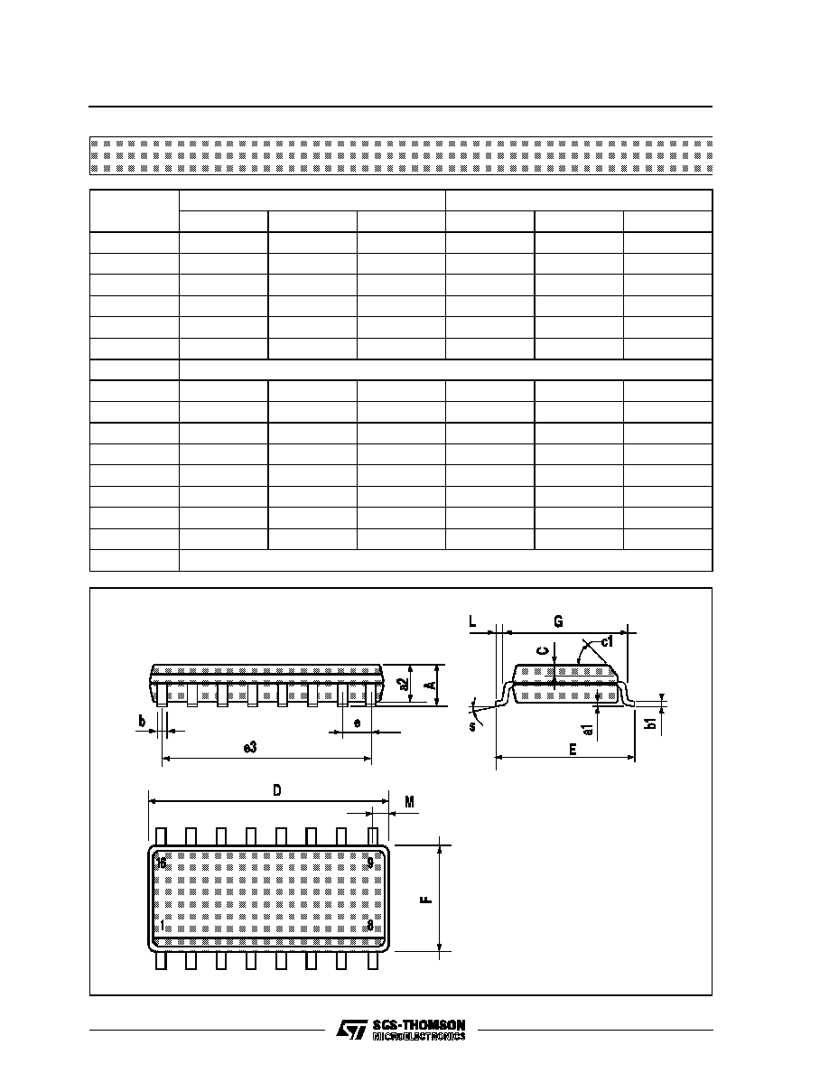
SO16 (Narrow) MECHANICAL DATA
DIM.
mm
inch
MIN.
TYP.
MAX.
MIN.
TYP.
MAX.
A
1.75
0.068
a1
0.1
0.2
0.004
0.007
a2
1.65
0.064
b
0.35
0.46
0.013
0.018
b1
0.19
0.25
0.007
0.010
C
0.5
0.019
c1
45
∞
(typ.)
D
9.8
10
0.385
0.393
E
5.8
6.2
0.228
0.244
e
1.27
0.050
e3
8.89
0.350
F
3.8
4.0
0.149
0.157
G
4.6
5.3
0.181
0.208
L
0.5
1.27
0.019
0.050
M
0.62
0.024
S
8
∞
(max.)
P013H
HCC/HCF4076B
11/13
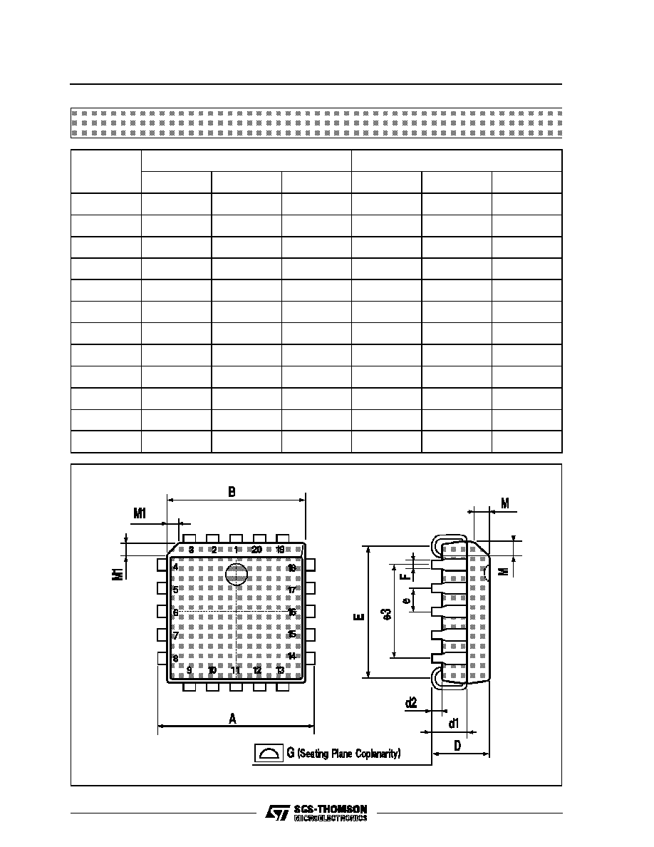
PLCC20 MECHANICAL DATA
DIM.
mm
inch
MIN.
TYP.
MAX.
MIN.
TYP.
MAX.
A
9.78
10.03
0.385
0.395
B
8.89
9.04
0.350
0.356
D
4.2
4.57
0.165
0.180
d1
2.54
0.100
d2
0.56
0.022
E
7.37
8.38
0.290
0.330
e
1.27
0.050
e3
5.08
0.200
F
0.38
0.015
G
0.101
0.004
M
1.27
0.050
M1
1.14
0.045
P027A
HCC/HCF4076B
12/13
Information furnished is believed to be accurate and reliable. However, SGS-THOMSON Microelectronics assumes no responsability for the
consequences of use of such information nor for any infringement of patents or other rights of third parties which may results from its use. No
license is granted by implication or otherwise under any patent or patent rights of SGS-THOMSON Microelectronics. Specifications mentioned
in this publication are subject to change without notice. This publication supersedes and replaces all information previously supplied.
SGS-THOMSON Microelectronics products are not authorized for use as critical components in life support devices or systems without express
written approval of SGS-THOMSON Microelectonics.
©
1994 SGS-THOMSON Microelectronics - All Rights Reserved
SGS-THOMSON Microelectronics GROUP OF COMPANIES
Australia - Brazil - France - Germany - Hong Kong - Italy - Japan - Korea - Malaysia - Malta - Morocco - The Netherlands -
Singapore - Spain - Sweden - Switzerland - Taiwan - Thailand - United Kingdom - U.S.A
HCC/HCF4076B
13/13