HCC/HCF4094B
8≠STAGE SHIFT-AND-STORE BUS REGISTER
DESCRIPTION
.
3-STATE PARALLEL OUTPUTS FOR CON-
NECTION TO COMMON BUS
.
SEPARATE
SERIAL
OUTPUTS
SYN-
CHRONOUS TO BOTH POSITIVE AND NEGA-
TIVE CLOCK EDGES FOR CASCADING
.
MEDIUM SPEED OPERATION 5MHz AT 10V
.
STANDARDIZED
SYMMETRICAL
OUTPUT
CHARACTERISTICS
.
QUIESCENT CURRENT SPECIFIED TO 20V
FOR HCC DEVICE
.
5V, 10V, AND 15V PARAMETRIC RATINGS
.
INPUT CURRENT OF 100nA AT 18V AND 25
∞
C
FOR HCC DEVICE
.
100% TESTED FOR QUIESCENT CURRENT
.
MEETS ALL REQUIREMENTS OF JEDEC TEN-
TATIVE STANDARD N
∞
. 13A, "STANDARD
SPECIFICATIONS FOR DESCRIPTION OF "B"
SERIES CMOS DEVICES"
June 1989
The HCC4094B (extended temperature range) and
HCF4094B (intermediate temperature range) are
monolithic integrated circuits available in 16-lead
dual in-line plastic or ceramic packageand plastic
micropackage.
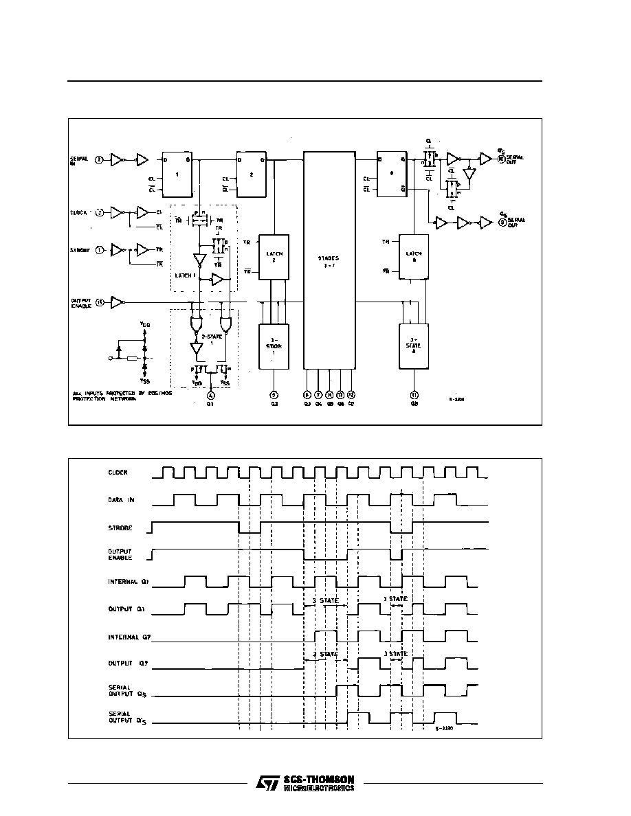
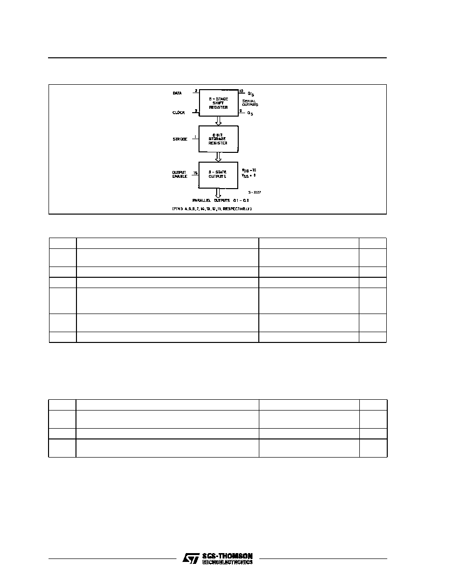
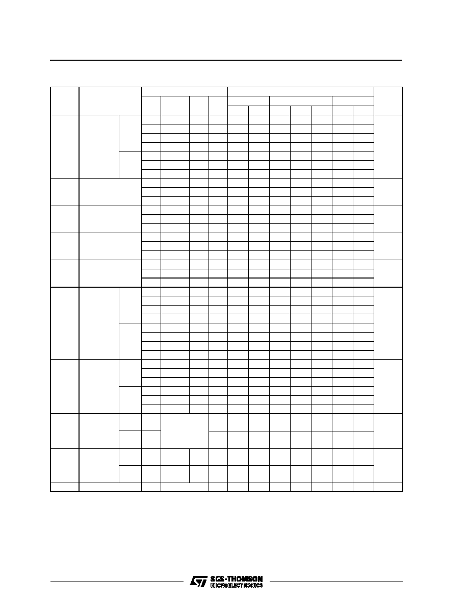
The HCC/HCF4094B is an 8-stage serial shift reg-
ister having a storage latch associated with each
stage for strobing data from the serial input to par-
allel buffered 3-state outputs. The parallel outputs
may be connected directly to common bus lines.
Data is shifted on positive clock transitions. The data
in each shift register stage is transferred to the stor-
age register when the STROBE input is high. Data
in the storage register appears at the outputs when-
ever the OUTPUT-ENABLE signal is high. Two ser-
ial outputs are available for cascading a number of
HCC/HCF4094B devices. Data is available at the
Q
S
serial output terminal on positive clock edges to
allow for high-speed operation in cascaded systems
in which the clock rise time is fast. The same serial
information, available at the Q'
S
terminal on the next
negative clock edge, provides a means for cascad-
ing HCC/HCF4094B devices when the clock rise
time is slow.
EY
(Plastic Package)
F
(Ceramic Frit Seal Package)
C1
(Plastic Chip Carrier)
ORDER CODES :
HCC4094BF
HCF4094BM1
HCF4094BEY
HCF4094BC1
PIN CONNECTIONS
M1
(Micro Package)
1/14
FUNCTIONAL DIAGRAM
ABSOLUTE MAXIMUM RATINGS
Symbol
Parameter
Value
Unit
V
DD
*
Supply Voltage : H CC Types
H C F Types
≠ 0.5 to + 20
≠ 0.5 to + 18
V
V
V
i
Input Voltage
≠ 0.5 to V
DD
+ 0.5
V
I
I
DC Input Current (any one input)
±
10
mA
P
t o t
Total Power Dissipation (per package)
Dissipation per Output Transistor
for T
o p
= Full Package-temperature Range
200
100
mW
mW
T
o p
Operating Temperature : HCC Types
H CF Types
≠ 55 to + 125
≠ 40 to + 85
∞
C
∞
C
T
st g
Storage Temperature
≠ 65 to + 150
∞
C
RECOMMENDED OPERATING CONDITIONS
Symbol
Parameter
Value
Unit
V
DD
Supply Voltage : HC C Types
H CF Types
3 to 18
3 to 15
V
V
V
I
Input Voltage
0 to V
DD
V
T
o p
Operating Temperature : HCC Types
H CF Types
≠ 55 to + 125
≠ 40 to + 85
∞
C
∞
C
Stresses above those listed under "Absolute Maximum Ratings" may cause permanent damage to the device. This is a stress rating only and
functional operation of the device at these or any other conditions above those indicated in the operational sections of this specification is not
implied. Exposure to absolute maximum rating conditions for external periods may affect device reliability.
* All voltage values are referred to V
SS
pin voltage.
HCC/HCF4094B
2/14
STATIC ELECTRICAL CHARACTERISTICS (over recommended operating conditions)
Test Conditions
Value
V
I
V
O
|I
O
|
V
D D
T
L o w
*
25
∞
C
T
Hi g h
*
Symbol
Parameter
(V)
(V)
(
µ
A)
(V)
Min. Max. Min. Typ. Max. Min. Max.
Unit
I
L
Quiescent
Current
HCC
Types
0/ 5
5
5
0.04
5
150
µ
A
0/10
10
10
0.04
10
300
0/15
15
20
0.04
20
600
0/20
20
100
0.08
100
3000
HCF
Types
0/ 5
5
20
0.04
20
150
0/10
10
40
0.04
40
300
0/15
15
80
0.04
80
600
V
O H
Output High
Voltage
0/ 5
< 1
5
4.95
4.95
4.95
V
0/10
< 1
10
9.95
9.95
9.95
0/15
< 1
15
14.95
14.95
14.95
V
O L
Output Low
Voltage
5/0
< 1
5
0.05
0.05
0.05
V
10/0
< 1
10
0.05
0.05
0.05
15/0
< 1
15
0.05
0.05
0.05
V
IH
Input High
Voltage
0.5/4.5
< 1
5
3.5
3.5
3.5
V
1/9
< 1
10
7
7
7
1.5/13.5
< 1
15
11
11
11
V
IL
Input Low
Voltage
4.5/0.5
< 1
5
1.5
1.5
1.5
V
9/1
< 1
10
3
3
3
13.5/1.5
< 1
15
4
4
4
I
O H
Output
Drive
Current
HCC
Types
0/ 5
2.5
5
≠ 2
≠ 1.6 ≠ 3.2
≠ 1.15
mA
0/ 5
4.6
5
≠ 0.64
≠ 0.51 ≠ 1
≠ 0.36
0/10
9.5
10
≠ 1.6
≠ 1.3 ≠ 2.6
≠ 0.9
0/15
13.5
15
≠ 4.2
≠ 3.4 ≠ 6.8
≠ 2.4
HCF
Types
0/ 5
2.5
5
≠ 1.53
≠ 1.36 ≠ 3.2
≠ 1.1
0/ 5
4.6
5
≠ 0.52
≠ 0.44 ≠ 1
≠ 0.36
0/10
9.5
10
≠ 1.3
≠ 1.1 ≠ 2.6
≠ 0.9
0/15
13.5
15
≠ 3.6
≠ 3.0 ≠ 6.8
≠ 2.4
I
O L
Output
Sink
Current
HCC
Types
0/ 5
0.4
5
0.64
0.51
1
0.36
mA
0/10
0.5
10
1.6
1.3
2.6
0.9
0/15
1.5
15
4.2
3.4
6.8
2.4
HCF
Types
0/ 5
0.4
5
0.52
0.44
1
0.36
0/10
0.5
10
1.3
1.1
2.6
0.9
0/15
1.5
15
3.6
3.0
6.8
2.4
I
IH
, I
IL
Input
Leakage
Current
HCC
Types
0/18
Any Input
18
±
0.1
±
10
≠ 5
±
0.1
±
1
µ
A
HCF
Types
0/15
15
±
0.3
±
10
≠ 5
±
0.3
±
1
I
O H
, I
O L
3-state
Output
Leakage
Current
HCC
Types
0/18
0/18
18
±
0.4
±
10
-4
±
0.4
±
12
µ
A
HCF
Types
0/15
0/15
15
±
1.0
±
10
- 4
±
1.0
±
7.5
C
I
Input Capacitance
Any Input
5
7.5
pF
* T
Low
= ≠ 55
∞
C for HCC device : ≠ 40
∞
C for HCF device.
* T
High
= + 125
∞
C for HCC device : + 85
∞
C for HCF device.
The Noise Margin for both "1" and "0" level is : 1V min. with V
DD
= 5V, 2V min. with V
DD
= 10V, 2.5V min. with V
DD
= 15V.
HCC/HCF4094B
5/14