 | –≠–ª–µ–∫—Ç—Ä–æ–Ω–Ω—ã–π –∫–æ–º–ø–æ–Ω–µ–Ω—Ç: HCC4099B | –°–∫–∞—á–∞—Ç—å:  PDF PDF  ZIP ZIP |
HCC/HCF4099B
September 1988
8-BIT ADDRESSABLE LATCH
.
SERIAL DATA INPUT - ACTIVE PARALLEL
OUTPUT
.
STORAGE REGISTER CAPABILITY - MASTER
CLEAR
.
CAN FUNCTION AS DEMULTIPLEXER
.
STANDARDIZED
SYMMETRICAL
OUTPUT
CHARACTERISTICS
.
QUIESCENT CURRENT SPECIFIED TO 20V
FOR HCC DEVICE
.
5V, 10V, AND 15V PARAMETRIC RATINGS
.
INPUT CURRENT OF 100nA AT 18V AND 25
∞
C
FOR HCC DEVICE
.
100% TESTED FOR QUIESCENT CURRENT
.
MEETS ALL REQUIREMENTS OF JEDEC TEN-
TATIVE STANDARD N
∞
. 13A, "STANDARD
SPECIFICATIONS FOR DESCRIPTION OF "B"
SERIES CMOS DEVICES"
DESCRIPTION
The HCC4099B (extended temperature range) and
HCF4099B (intermediate temperature range) are
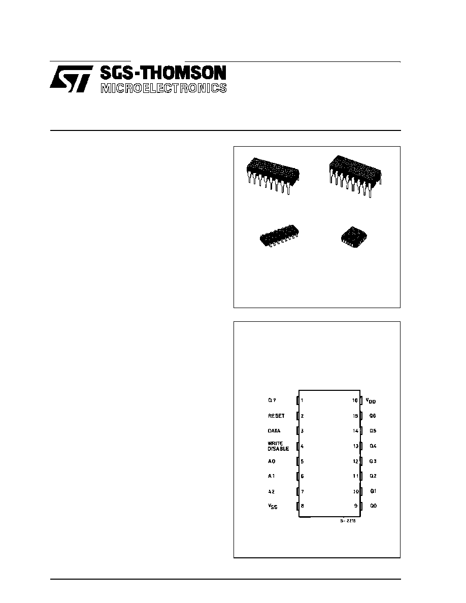
monolithic integrated circuits, available in 16-lead dual
in-line plastic or ceramic package and plastic micro
package. The HCC/HCF4099B 8-bit addressable
latch is a serial-input, parallel-output storage register
that can perform a variety of functions. Data are in-
putted to a particular bit in the latch when that bit is
addressed (by means of inputs A0, A1, A2) and
when WRITE DISABLE is at a low level. When
WRITE DISABLE is high, data entry is inhibited ;
however, all 8 outputs can be continuously read in-
dependent of WRITE DISABLE and address inputs.
A master RESET input is available, which resets all
bits to a logic "0" level when RESET and WRITE
DISABLE are at a high level. When RESET is at a
high level, and WRITE DISABLE is at a low level, the
latch acts as a 1-of-8 demultiplexer ; the bit that is
addressed has an active output which follows the
data input, while all unaddressed bits are held to a
logic "0" level.
ORDER CODES :
HCC4099BF
HCF4099BM1
HCF4099BEY
HCF4099BC1
M1
Micro Package
C1
Plastic Chip Carrier
EY
Plastic Package
F
Ceramic Frit Seal Package
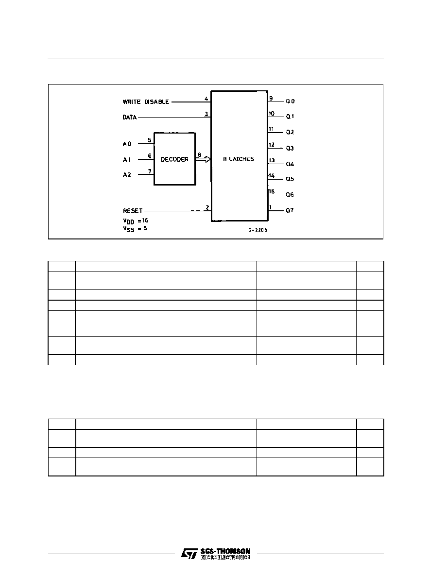
PIN CONNECTIONS
1/14
FUNCTIONAL DIAGRAM
ABSOLUTE MAXIMUM RATINGS
Symbol
Parameter
Value
Unit
V
DD
*
Supply Voltage : HC C Types
H C F Types
≠ 0.5 to + 20
≠ 0.5 to + 18
V
V
V
i
Input Voltage
≠ 0.5 to V
DD
+ 0.5
V
I
I
DC Input Current (any one input)
±
10
mA
P
t o t
Total Power Dissipation (per package)
Dissipation per Output Transistor
for T
o p
= Full Package-temperature Range
200
100
mW
mW
T
o p
Operating Temperature : HCC Types
H CF Types
≠ 55 to + 125
≠ 40 to + 85
∞
C
∞
C
T
s t g
Storage Temperature
≠ 65 to + 150
∞
C
Stresses above listed under "Absolute Maximum Ratings" may cause permanent damage to the device. This is a stress rating only and
functional operation of the device at these or any other conditions above those indicated in the operational sections of this specification is
not implied. Exposure to absolute maximum rating conditions for external periods may affect device reliability.
* All voltage values are referred to V
SS
pin voltage.
RECOMMENDED OPERATING CONDITIONS
Symbol
Parameter
Value
Unit
V
DD
Supply Voltage : HCC Types
H CF Types
3 to 18
3 to 15
V
V
V
I
Input Voltage
0 to V
DD
V
T
o p
Operating Temperature : HCC Types
HC F Types
≠ 55 to + 125
≠ 40 to + 85
∞
C
∞
C
HCC/HCF4099B
2/14
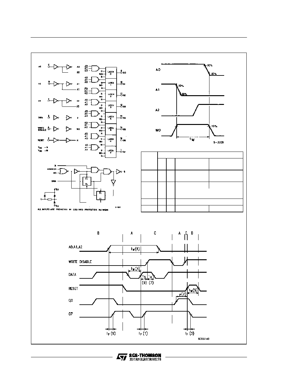
LOGIC DIAGRAM
Definition of WRITE DIABLE ON Time
Mode Selection
Types
W D R
Addressed
Latch
Unaddressed
Latch
A
0
0
Follows Data
Holds Previous
State
B
0
1
Follows Data
Reset to "0"
(active high 8-channel
demultiplexer)
C
1
0
Holds Previous State
D
1
1
Reset to "0"
Reset to "0"
WD = WRITE DISABLE
R = RESET
1 of 8 latches
Master Timing Diagram
HCC/HCF4099B
3/14
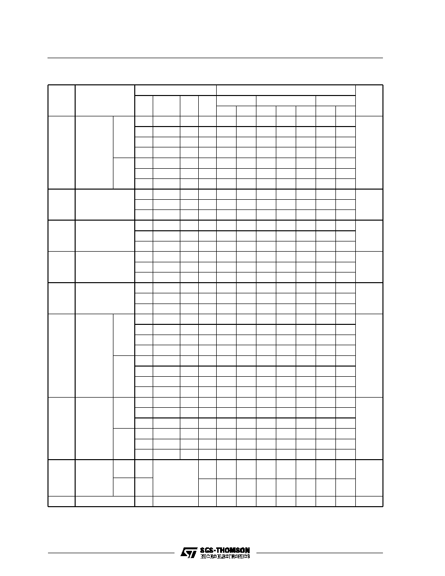
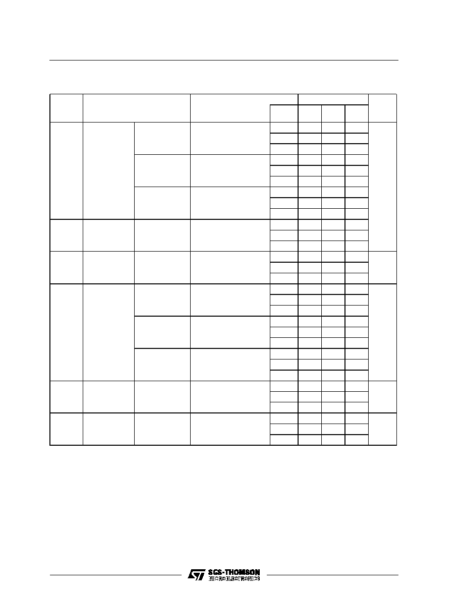
STATIC ELECTRICAL CHARACTERISTICS (over recommended operating conditions)
Test Conditions
Value
V
I
V
O
|I
O
|
V
D D
T
L o w
*
25
∞
C
T
Hi g h
*
Symbol
Parameter
(V)
(V)
(
µ
A)
(V)
Min. Max. Min. Typ. Max. Min. Max.
Unit
I
L
Quiescent
Current
HCC
Types
0/ 5
5
5
0.04
5
150
µ
A
0/10
10
10
0.04
10
300
0/15
15
20
0.04
20
600
0/20
20
100
0.08
100
3000
HCF
Types
0/ 5
5
20
0.04
20
150
0/10
10
40
0.04
40
300
0/15
15
80
0.04
80
600
V
O H
Output High
Voltage
0/ 5
< 1
5
4.95
4.95
4.95
V
0/10
< 1
10
9.95
9.95
9.95
0/15
< 1
15
14.95
14.95
14.95
V
O L
Output Low
Voltage
5/0
< 1
5
0.05
0.05
0.05
V
10/0
< 1
10
0.05
0.05
0.05
15/0
< 1
15
0.05
0.05
0.05
V
IH
Input High
Voltage
0.5/4.5
< 1
5
3.5
3.5
3.5
V
1/9
< 1
10
7
7
7
1.5/13.5
< 1
15
11
11
11
V
IL
Input Low
Voltage
4.5/0.5
< 1
5
1.5
1.5
1.5
V
9/1
< 1
10
3
3
3
13.5/1.5
< 1
15
4
4
4
I
O H
Output
Drive
Current
HCC
Types
0/ 5
2.5
5
≠ 2
≠ 1.6 ≠ 3.2
≠ 1.15
mA
0/ 5
4.6
5
≠ 0.64
≠ 0.51 ≠ 1
≠ 0.36
0/10
9.5
10
≠ 1.6
≠ 1.3 ≠ 2.6
≠ 0.9
0/15
13.5
15
≠ 4.2
≠ 3.4 ≠ 6.8
≠ 2.4
HCF
Types
0/ 5
2.5
5
≠ 1.53
≠ 1.36 ≠ 3.2
≠ 1.1
0/ 5
4.6
5
≠ 0.52
≠ 0.44 ≠ 1
≠ 0.36
0/10
9.5
10
≠ 1.3
≠ 1.1 ≠ 2.6
≠ 0.9
0/15
13.5
15
≠ 3.6
≠ 3.0 ≠ 6.8
≠ 2.4
I
O L
Output
Sink
Current
HCC
Types
0/ 5
0.4
5
0.64
0.51
1
0.36
mA
0/10
0.5
10
1.6
1.3
2.6
0.9
0/15
1.5
15
4.2
3.4
6.8
2.4
HCF
Types
0/ 5
0.4
5
0.52
0.44
1
0.36
0/10
0.5
10
1.3
1.1
2.6
0.9
0/15
1.5
15
3.6
3.0
6.8
2.4
I
IH
, I
IL
Input
Leakage
Current
HCC
Types
0/18
Any Input
18
±
0.1
±
10
≠ 5
±
0.1
±
1
µ
A
HCF
Types
0/15
15
±
0.3
±
10
≠ 5
±
0.3
±
1
C
I
Input Capacitance
Any Input
5
7.5
pF
* T
LOW
= ≠ 55
∞
C for HCC device : ≠ 40
∞
C for HCF device.
* T
HIGH
= + 125
∞
C for HCC device : + 85
∞
C for HCF device.
The Noise Margin for both "1" and "0" level is : 1V min. with V
DD
= 5V, 2V min. with V
DD
= 10V, 2.5V min. with V
DD
= 15V,
HCC/HCF4099B
4/14
DYNAMIC ELECTRICAL CHARACTERISTICS (T
am b
= 25
∞
C, C
L
= 50pF, R
L
= 200k
,
typical temperature coefficient for all V
D D
values is 0.3%/
∞
C, all input rise and fall times = 20ns)
Val ue
Symbol
Parameter
Test Conditions
(see master timing
diagram)
V
D D
(V) Min.
Typ.
Max.
Unit
t
PL H
, t
P HL
Propagation
Delay Time
Data to Output
(1)
5
200
400
ns
10
75
150
15
50
100
Write Disable to
Output
(2)
5
200
400
10
80
160
15
60
120
Address to
Output
(9)
5
225
450
10
100
200
15
75
150
t
PHL
Propagation
Delay Time
Reset to Output
(3)
5
175
350
10
80
160
15
65
130
t
THL
, t
T L H
Transition
Time
Any Output
5
100
200
ns
10
50
100
15
40
80
t
W
Pulse Width
Data
(4)
5
200
100
ns
10
100
50
15
80
40
Address
(8)
5
400
200
10
200
100
15
125
65
Reset
(5)
5
150
75
10
75
40
15
50
25
t
s e t u p
Setup Time
Data to Write
Disable
(6)
5
100
50
ns
10
50
25
15
35
20
t
h o ld
Hold Time
Data to Write
Disable
(7)
5
150
75
ns
10
75
40
15
50
25
HCC/HCF4099B
5/14
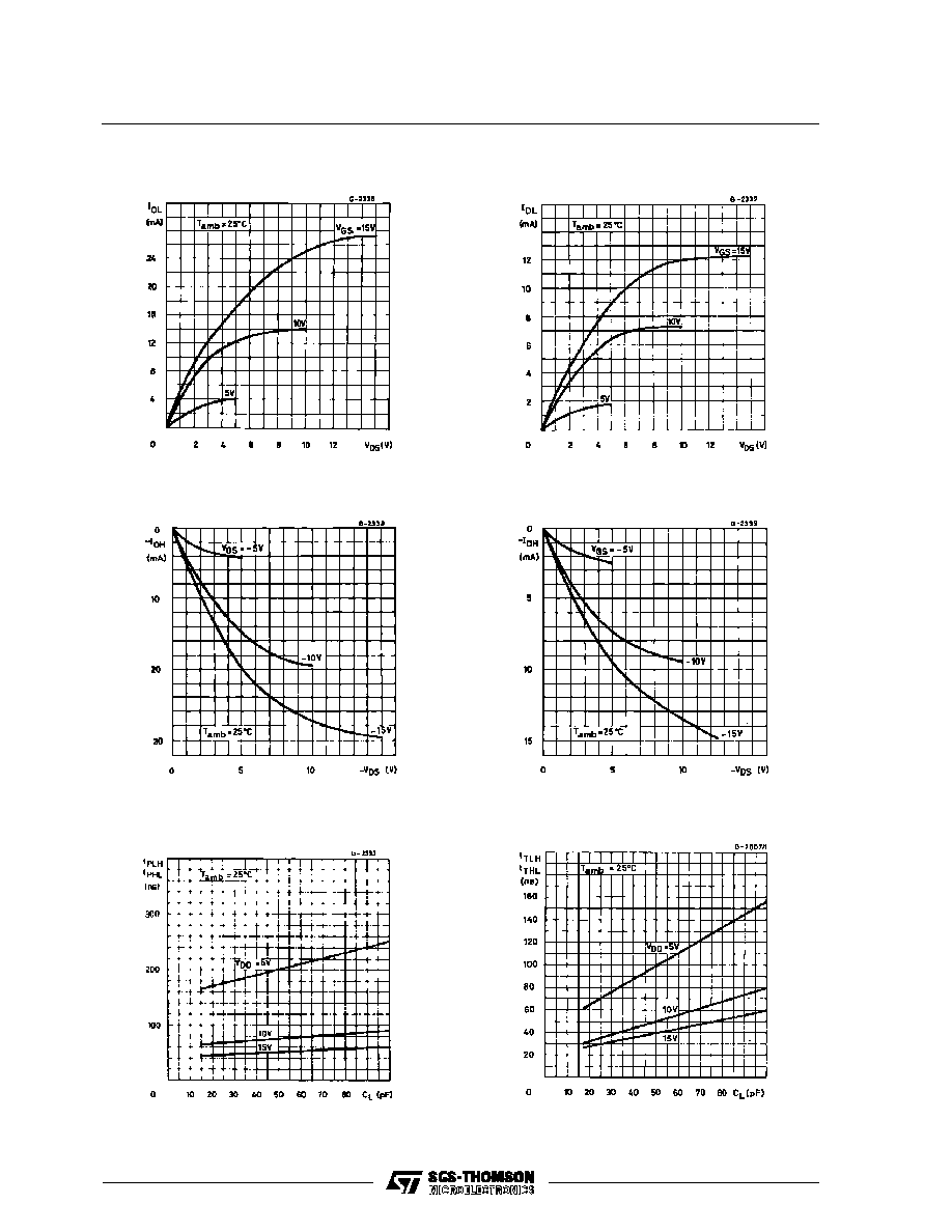
Minimum Output Low (sink) Current Charac-
teristics.
Typical Output High (source) Current Charac-
teristics.
Minimum Output High (source) Current Charac-
teristics.
Typical Propagation Delay Time (data to Qn) vs.
Load Capacitance.
Typical Transition Time vs. Load Capacitance.
Typical Output Low (sink) Current Characteristics.
HCC/HCF4099B
6/14
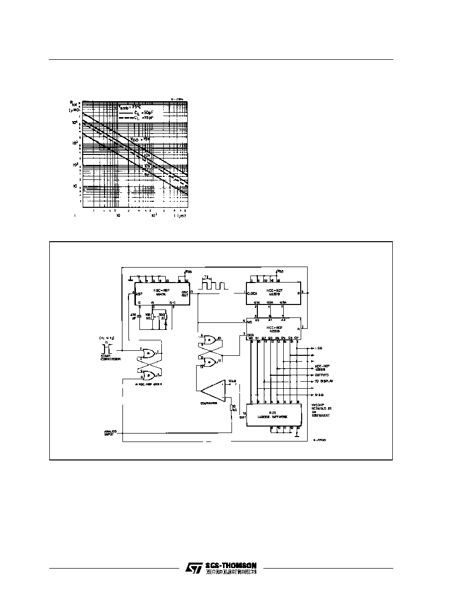
Typical Dynamic power Dissipation vs. Address
Cycle Time.
TYPICAL APPLICATIONS
A/D Converter
HCC/HCF4099B
7/14
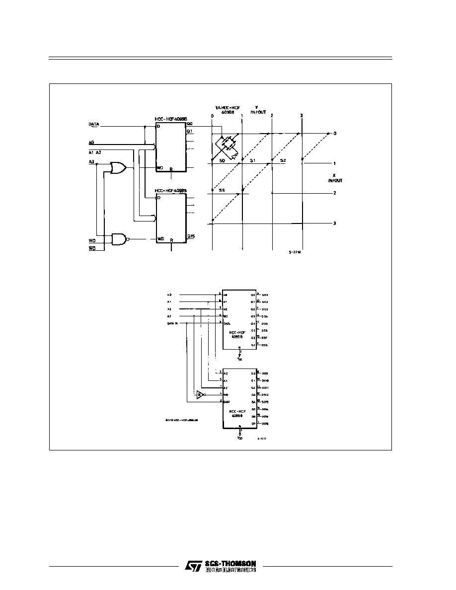
TYPICAL APPLICATIONS
Multiple Selection Decoding ≠ 4x4 Crosspoint Switch
1 of 16 Decoder/demultiplexer
HCC/HCF4099B
8/14
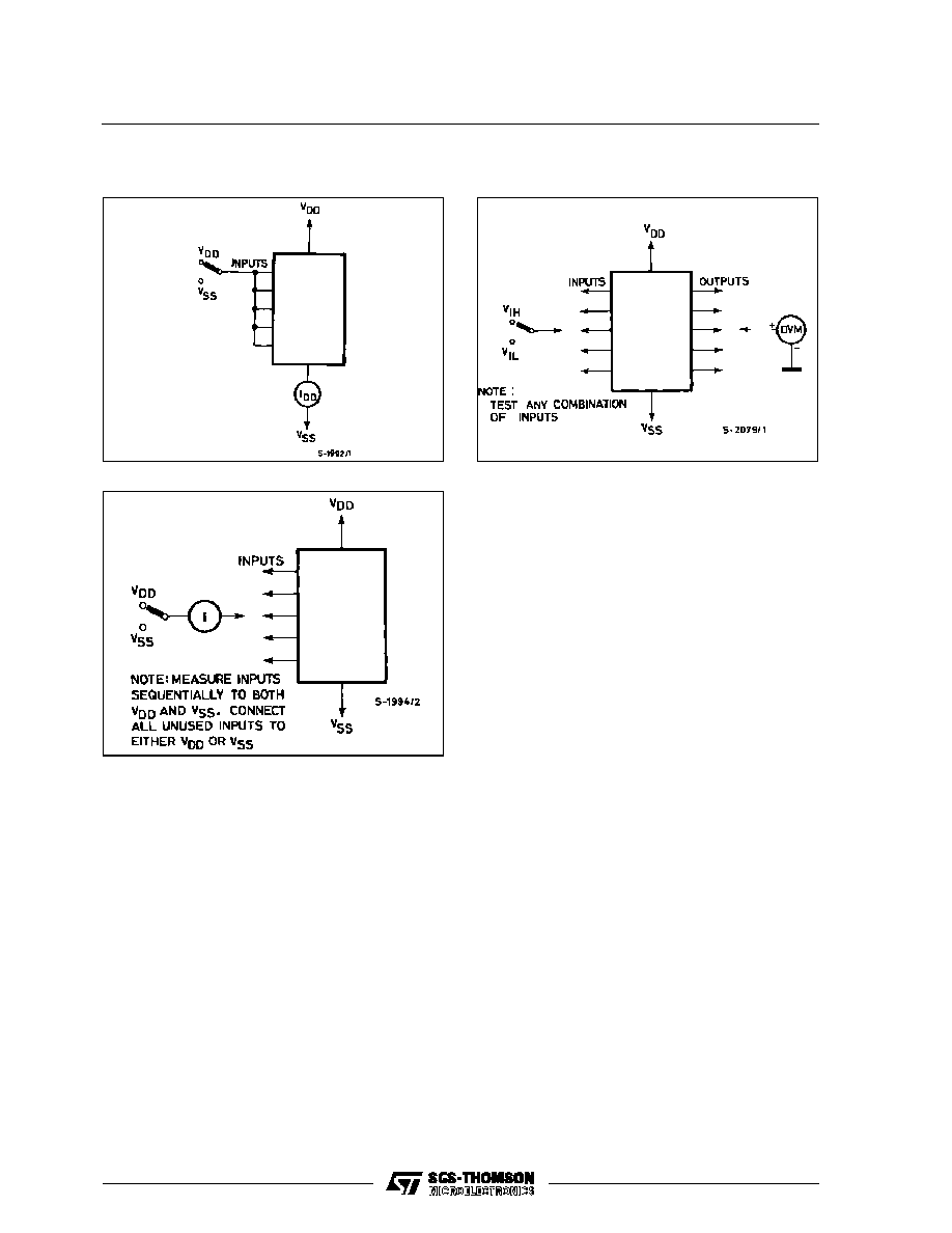
TEST CIRCUITS
Input Voltage.
Quiescent Device Current.
Input Current.
HCC/HCF4099B
9/14

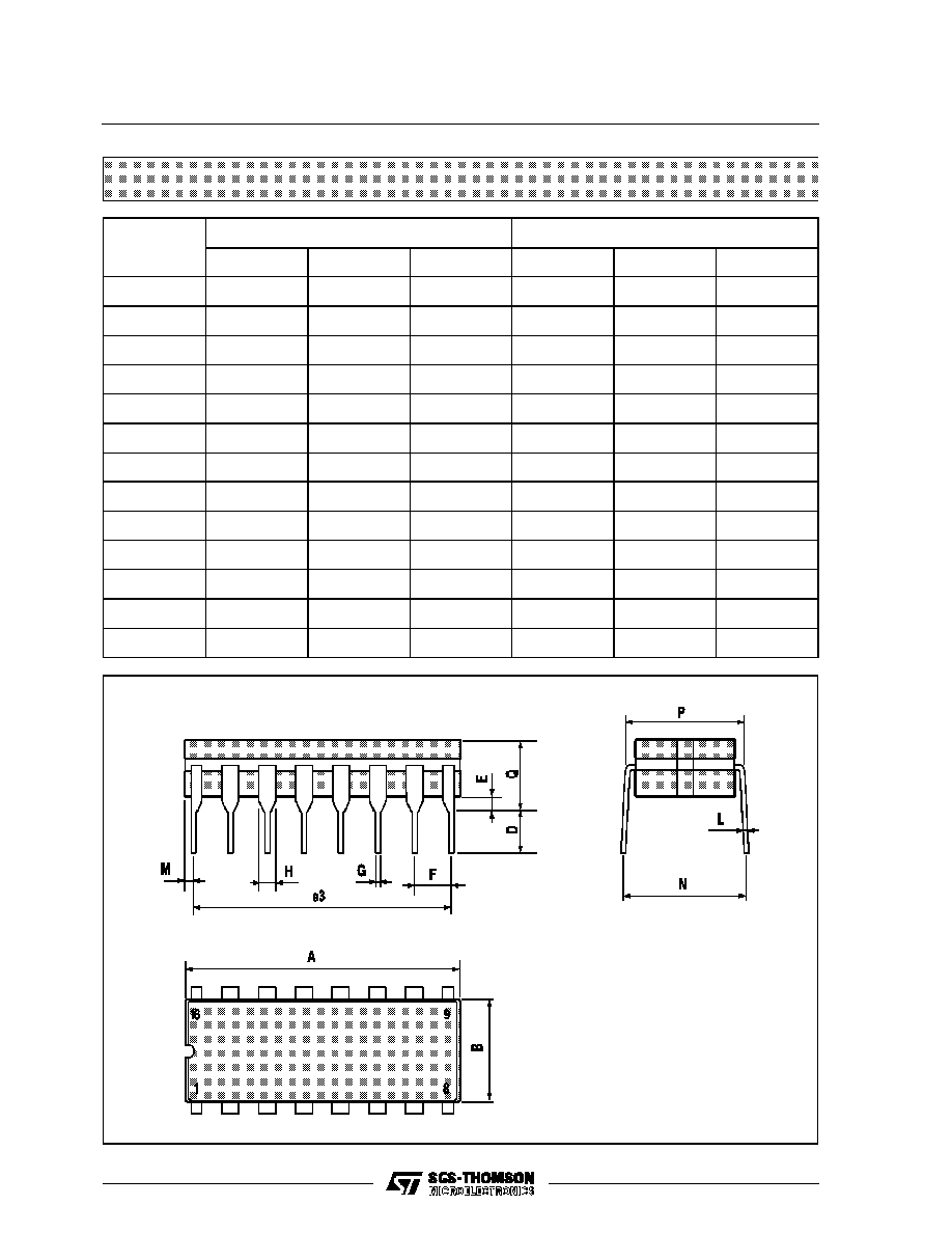
Plastic DIP16 (0.25) MECHANICAL DATA
DIM.
mm
inch
MIN.
TYP.
MAX.
MIN.
TYP.
MAX.
a1
0.51
0.020
B
0.77
1.65
0.030
0.065
b
0.5
0.020
b1
0.25
0.010
D
20
0.787
E
8.5
0.335
e
2.54
0.100
e3
17.78
0.700
F
7.1
0.280
I
5.1
0.201
L
3.3
0.130
Z
1.27
0.050
P001C
HCC/HCF4099B
10/14
Ceramic DIP16/1 MECHANICAL DATA
DIM.
mm
inch
MIN.
TYP.
MAX.
MIN.
TYP.
MAX.
A
20
0.787
B
7
0.276
D
3.3
0.130
E
0.38
0.015
e3
17.78
0.700
F
2.29
2.79
0.090
0.110
G
0.4
0.55
0.016
0.022
H
1.17
1.52
0.046
0.060
L
0.22
0.31
0.009
0.012
M
0.51
1.27
0.020
0.050
N
10.3
0.406
P
7.8
8.05
0.307
0.317
Q
5.08
0.200
P053D
HCC/HCF4099B
11/14

SO16 (Narrow) MECHANICAL DATA
DIM.
mm
inch
MIN.
TYP.
MAX.
MIN.
TYP.
MAX.
A
1.75
0.068
a1
0.1
0.2
0.004
0.007
a2
1.65
0.064
b
0.35
0.46
0.013
0.018
b1
0.19
0.25
0.007
0.010
C
0.5
0.019
c1
45
∞
(typ.)
D
9.8
10
0.385
0.393
E
5.8
6.2
0.228
0.244
e
1.27
0.050
e3
8.89
0.350
F
3.8
4.0
0.149
0.157
G
4.6
5.3
0.181
0.208
L
0.5
1.27
0.019
0.050
M
0.62
0.024
S
8
∞
(max.)
P013H
HCC/HCF4099B
12/14
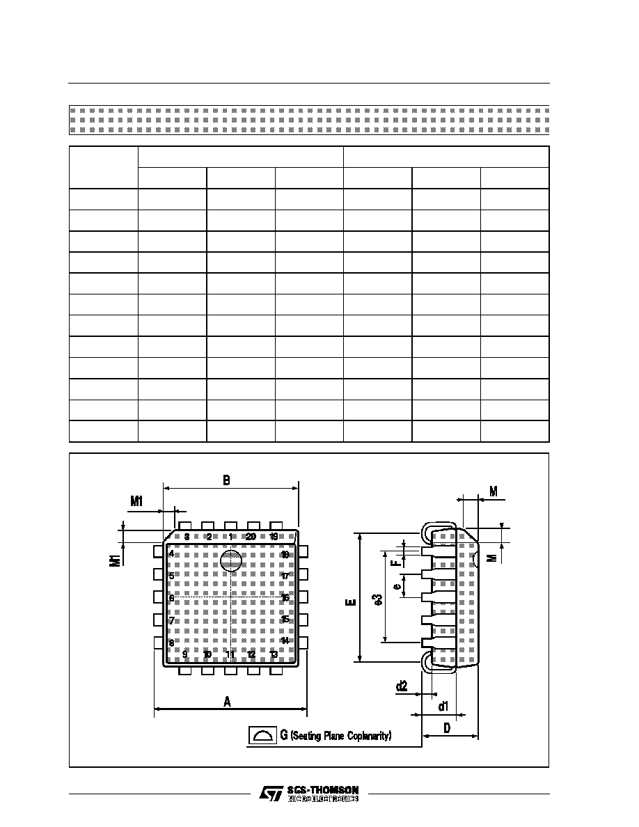
PLCC20 MECHANICAL DATA
DIM.
mm
inch
MIN.
TYP.
MAX.
MIN.
TYP.
MAX.
A
9.78
10.03
0.385
0.395
B
8.89
9.04
0.350
0.356
D
4.2
4.57
0.165
0.180
d1
2.54
0.100
d2
0.56
0.022
E
7.37
8.38
0.290
0.330
e
1.27
0.050
e3
5.08
0.200
F
0.38
0.015
G
0.101
0.004
M
1.27
0.050
M1
1.14
0.045
P027A
HCC/HCF4099B
13/14

Information furnished is believed to be accurate and reliable. However, SGS-THOMSON Microelectronics assumes no responsability for the
consequences of use of such information nor for any infringement of patents or other rights of third parties which may results from its use. No
license is granted by implication or otherwise under any patent or patent rights of SGS-THOMSON Microelectronics. Specifications mentioned
in this publication are subject to change without notice. This publication supersedes and replaces all information previously supplied.
SGS-THOMSON Microelectronics products are not authorized for use as critical components in life support devices or systems without express
written approval of SGS-THOMSON Microelectonics.
©
1994 SGS-THOMSON Microelectronics - All Rights Reserved
SGS-THOMSON Microelectronics GROUP OF COMPANIES
Australia - Brazil - France - Germany - Hong Kong - Italy - Japan - Korea - Malaysia - Malta - Morocco - The Netherlands -
Singapore - Spain - Sweden - Switzerland - Taiwan - Thailand - United Kingdom - U.S.A
HCC/HCF4099B
14/14