 | –≠–ª–µ–∫—Ç—Ä–æ–Ω–Ω—ã–π –∫–æ–º–ø–æ–Ω–µ–Ω—Ç: HCC4517BF | –°–∫–∞—á–∞—Ç—å:  PDF PDF  ZIP ZIP |
HCC/HCF4517B
September 1988
DUAL 64-STAGE STATIC SHIFT REGISTER
.
CLOCK FREQUENCY 12MHz (TYP.) AT V
DD
=
10V
.
SCHMITT TRIGGER CLOCK INPUTS ALLOW
OPERATION WITH VERY SLOW CLOCK RISE
AND FALL TIMES
.
THREE-STATE OUTPUTS
.
QUIESCENT CURRENT SPECIFIED AT 20V
FOR HCC DEVICE
.
STANDARDIZED, SYMMETRICAL OUTPUT
CHARACTERISTICS
.
5V, 10V, AND 15V PARAMETRIC RATINGS
.
INPUT CURREN OF 100nA AT 18V AND 25
∞
C
FOR HCC DEVICE
.
100% TESTED FOR QUIESCENT CURRENT
.
MEETS ALL REQUIREMENTS OF JEDEC TEN-
TATIVE STANDARD N
∞
. 13A, "STANDARD
SPECIFICATIONS FOR DESCRIPTION OF "B"
SERIES CMOS DEVICES"
DESCRIPTION
The HCC4517B (extended temperature range) and
HCF4517B (intermediate temperature range) are
monolithic integrated circuits, available in 16-lead
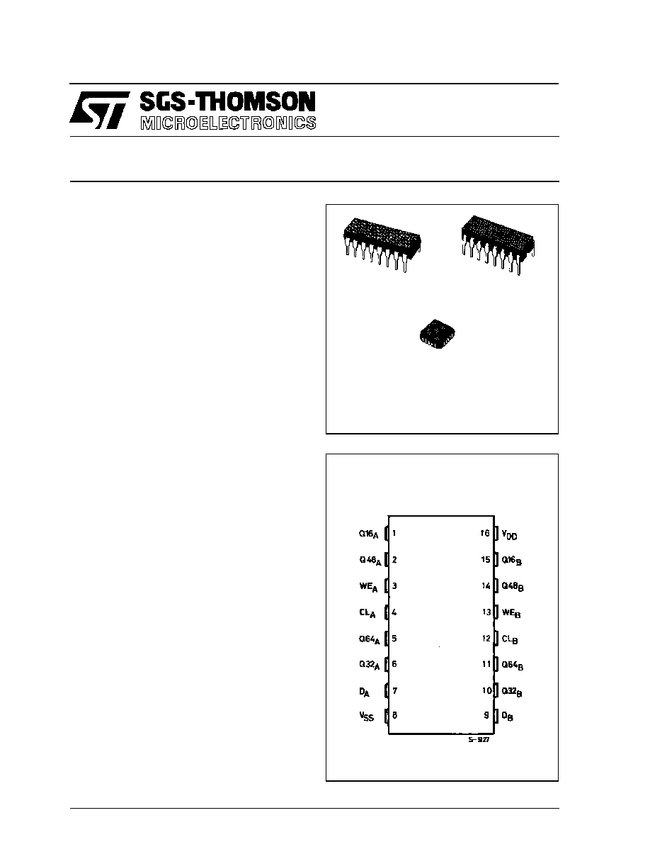
dual in-line plastic or ceramic package.
The HCC/HCF4517B dual 64-stage static shift reg-
ister consists of two independent registers each
having a clock, data, and write enable input and out-
puts accessible at taps following the 16th, 32nd,
48th, and 64th stages. These taps also serve as
input points allowing data to be inputted at the 17th,
33rd, and 49th stages when the write enable input
is a logic 1 and the clock goes through a low-to-high
transition. The truth table indicates how the clock
and write enable inputs control the operation of the
HCC/HCF4517B. Inputs at the intermediate taps
allow entry of 64 bits into the register with 16 clock
pulses. The 3-state outputs permit connection of this
device to an external bus.
EY
(Plastic Package)
F
(Ceramic Package)
C1
(Chip Carrier)
ORDER CODES :
HCC4517BF
HCF4517BM1
HCF4517BC1
PIN CONNECTIONS
1/12

Stresses above those listed under "Absolute Maximum Ratings" may cause permanent damage to the device. This is a stress
rating only and functional operation of the device at these or any other conditions above those indicated in the operational sections
of this specification is not implied. Exposure to absolute maximum rating conditions for extended periods may affect device reliability.
* All voltages are with respect to V
SS
(GND).
ABSOLUTE MAXIMUM RATINGS
Symbol
Parameter
Value
Unit
V
DD
*
Supply Voltage : HC C Types
H C F Types
≠ 0.5 to + 20
≠ 0.5 to + 18
V
V
V
i
Input Voltage
≠ 0.5 to V
DD
+ 0.5
V
I
I
DC Input Current (any one input)
±
10
mA
P
t o t
Total Power Dissipation (per package)
Dissipation per Output Transistor
for T
o p
= Full Package-temperature Range
200
100
mW
mW
T
o p
Operating Temperature : HCC Types
H CF Types
≠ 55 to + 125
≠ 40 to + 85
∞
C
∞
C
T
s t g
Storage Temperature
≠ 65 to + 150
∞
C
RECOMMENDED OPERATING CONDITIONS
Symbol
Parameter
Val ue
Unit
V
DD
Supply Voltage : H CC Types
H C F Types
3 to 18
3 to 15
V
V
V
I
Input Voltage
0 to V
DD
V
T
o p
Operating Temperature : HC C Types
H CF Types
≠ 55 to + 125
≠ 40 to + 85
∞
C
∞
C
FUNCTIONAL DIAGRAM (one half)
HCC/HCF4517B
2/12
LOGIC DIAGRAM AND TRUTH TABLE
Clock
Write
Enable
D ata
Stage 1 6
T ap
Stage 3 2
T a p
Stage 4 8
Ta p
Stage 6 4
Ta p
0
0
X
Q16
Q32
Q48
Q64
0
1
X
Z
Z
Z
Z
1
0
X
Q16
Q32
Q48
Q64
1
1
X
Z
Z
Z
Z
≠
/
≠
0
DI In
Q16
Q32
Q48
Q64
≠
/
≠
1
Di In
D17 In
D33 In
D49 In
Z
≠
\≠
0
X
Q16
Q32
Q48
Q64
≠
\≠
1
X
Z
Z
Z
Z
HCC/HCF4517B
3/12
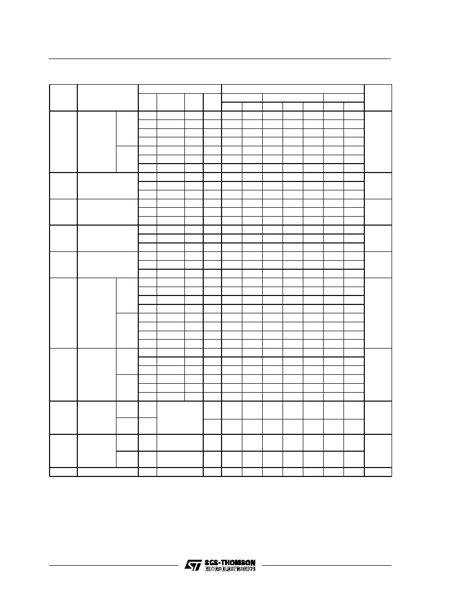
STATIC ELECTRICAL CHARACTERISTICS (over recommended operating conditions)
Test Conditions
Val ue
V
I
V
O
|I
O
|
V
D D
T
L o w
*
25
∞
C
T
Hi g h
*
Symbol
Parameter
(V)
(V)
(
µ
A)
(V)
Mi n. Max. Min. Typ. Max. Min. Max.
Unit
I
L
Quiescent
Current
HCC
Types
0/ 5
5
5
0.04
5
150
µ
A
0/10
10
10
0.04
10
300
0/15
15
20
0.04
20
600
0/20
20
100
0.08
100
3000
HCF
Types
0/ 5
5
20
0.04
20
150
0/10
10
40
0.04
40
300
0/15
15
80
0.04
80
600
V
O H
Output High
Voltage
0/ 5
< 1
5
4.95
4.95
4.95
V
0/10
< 1
10
9.95
9.95
9.95
0/15
< 1
15
14.95
14.95
14.95
V
O L
Output Low
Voltage
5/0
< 1
5
0.05
0.05
0.05
V
10/0
< 1
10
0.05
0.05
0.05
15/0
< 1
15
0.05
0.05
0.05
V
IH
Input High
Voltage
0.5/4.5
< 1
5
3.5
3.5
3.5
V
1/9
< 1
10
7
7
7
1.5/13.5
< 1
15
11
11
11
V
IL
Input Low
Voltage
4.5/0.5
< 1
5
1.5
1.5
1.5
V
9/1
< 1
10
3
3
3
13.5/1.5
< 1
15
4
4
4
I
O H
Output
Drive
Current
HCC
Types
0/ 5
2.5
5
≠ 2
≠ 1.6 ≠ 3.2
≠ 1.15
mA
0/ 5
4.6
5
≠ 0.64
≠ 0.51 ≠ 1
≠ 0.36
0/10
9.5
10
≠ 1.6
≠ 1.3 ≠ 2.6
≠ 0.9
0/15
13.5
15
≠ 4.2
≠ 3.4 ≠ 6.8
≠ 2.4
HCF
Types
0/ 5
2.5
5
≠ 1.53
≠ 1.36 ≠ 3.2
≠ 1.1
0/ 5
4.6
5
≠ 0.52
≠ 0.44 ≠ 1
≠ 0.36
0/10
9.5
10
≠ 1.3
≠ 1.1 ≠ 2.6
≠ 0.9
0/15
13.5
15
≠ 3.6
≠ 3.0 ≠ 6.8
≠ 2.4
I
O L
Output
Sink
Current
HCC
Types
0/ 5
0.4
5
0.64
0.51
1
0.36
mA
0/10
0.5
10
1.6
1.3
2.6
0.9
0/15
1.5
15
4.2
3.4
6.8
2.4
HCF
Types
0/ 5
0.4
5
0.52
0.44
1
0.36
0/10
0.5
10
1.3
1.1
2.6
0.9
0/15
1.5
15
3.6
3.0
6.8
2.4
I
IH
, I
IL
Input
Leakage
Current
HCC
Types
0/18
Any Input
18
±
0.1
±
10
≠ 5
±
0.1
±
1
µ
A
HCF
Types
0/15
15
±
0.3
±
10
≠ 5
±
0.3
±
1
I
O H
, I
O L
3-State
Output
Leakage
Current
HCC
Types
0/18
18
±
0.4
±
10
≠ 4
±
0.4
±
12
µ
A
HCF
Types
0/18
15
±
1.0
±
10
≠ 4
±
1.0
±
7.5
C
I
Input Capacitance
Any Input
5
7.5
pF
* T
Lo w
= ≠ 55
∞
C for HCC device : ≠ 40
∞
C for HCF device.
* T
High
= + 125
∞
C for HCC device : + 85
∞
C for HCF device.
The Noise Margin for both "1" and "0" level is : 1V min. with V
DD
= 5V, 2V min. with V
DD
= 10V, 2.5V min. with V
DD
= 15V,
HCC/HCF4517B
4/12
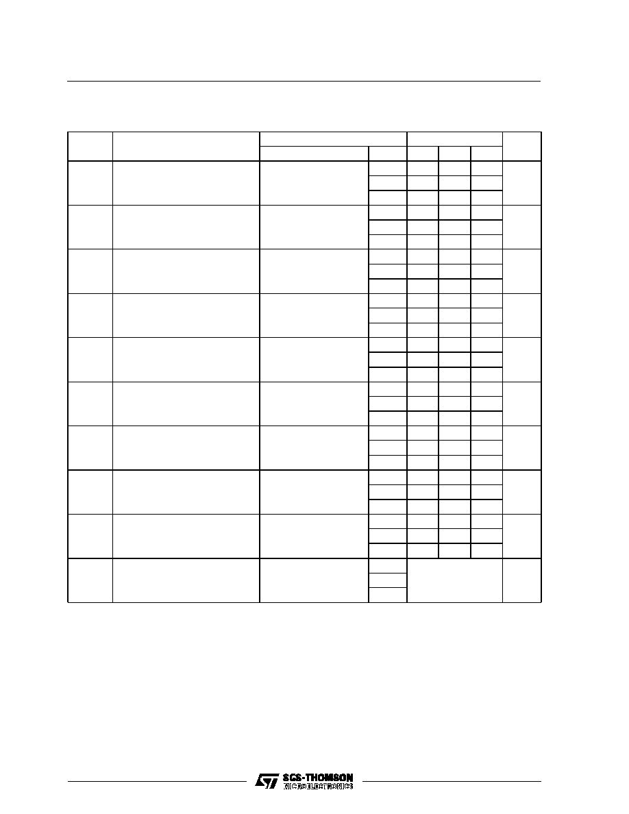
DYNAMIC ELECTRICAL CHARACTERISTICS (T
amb
= 25
∞
C, Input t
r
, t
f
= 20ns, C
L
= 50pF,
R
L
= 200k
)
Test Conditions
Val ue
Symbol
Parameter
V
D D
(V)
Min.
Typ.
Max.
Unit
t
P HL
, t
P L H
Propagation Delay Time :
CL to Bit 16 Tap
5
200
400
ns
10
110
220
15
90
180
t
PL Z
, t
P HZ
t
PZ L
, t
P ZH
3-State Output WE to Bit 16 Tap
(see note)
5
75
150
ns
10
40
80
15
30
60
t
THL
, t
T L H
Output Transition Time
5
100
200
ns
10
50
100
15
40
80
t
se t u p
Write Enable to Clock
5
≠ 100
≠ 50
ns
10
≠ 50
≠ 25
15
≠ 30
≠ 15
t
se t u p
Data to Clock
5
≠ 100
≠ 50
ns
10
≠ 60
≠ 30
15
≠ 30
≠ 15
Write Enable to Clock
Release Time
5
50
100
ns
10
25
50
15
20
40
t
h o ld
Data to Clock
5
100
200
ns
10
50
100
15
25
50
t
W
Minimum Clock Pulse Width
5
90
180
ns
10
40
80
15
25
50
f
CL
Maximum Clock Input
Frequency
5
3
6
MHz
10
6
12
15
8
15
t
f
, t
r
Maximum Clock Input Rise
or Fall Time
5
UNLIMITED
µ
s
10
15
Note : Measured at the point of 10% change in output load of 50pF, R
L
= 1k
to V
DD
for t
PZL
, t
PLZ
and R
L
= 1k
to V
SS
for t
PHZ.
HCC/HCF4517B
5/12
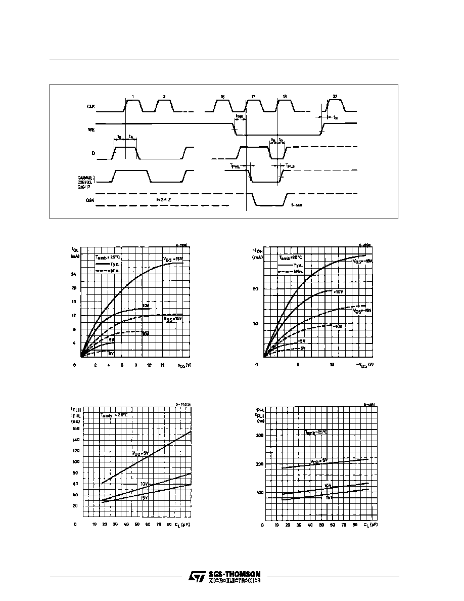
WAVEFORMS
Output Low (sink) Current Characteristics.
Output High (source) Current Characteristics.
Typical Propagation Delay Time vs. Load Capacit-
ance.
Typical Transition Time vs. Load Capacitance.
HCC/HCF4517B
6/12
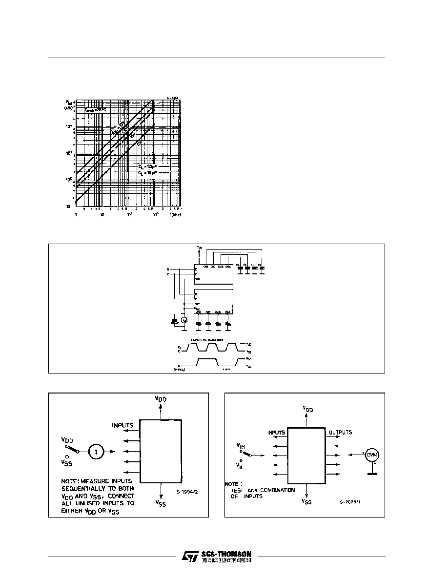
Typical Dynamic Power Dissipation vs. Fre-
quency.
Dynamic Power Dissipation and Waveforms.
TEST CIRCUITS
HCC/HCF4517B
7/12
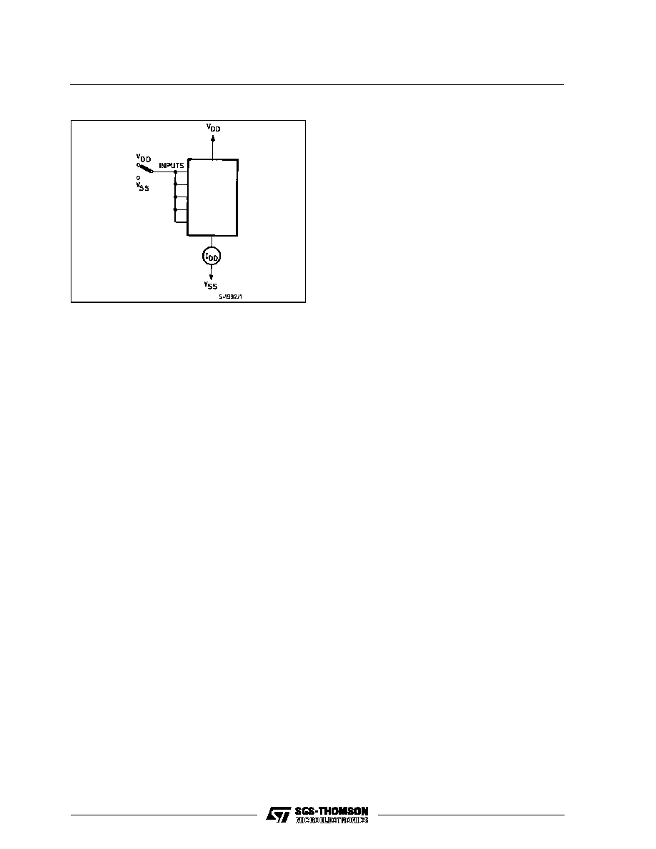
TEST CIRCUITS (continued)
HCC/HCF4517B
8/12
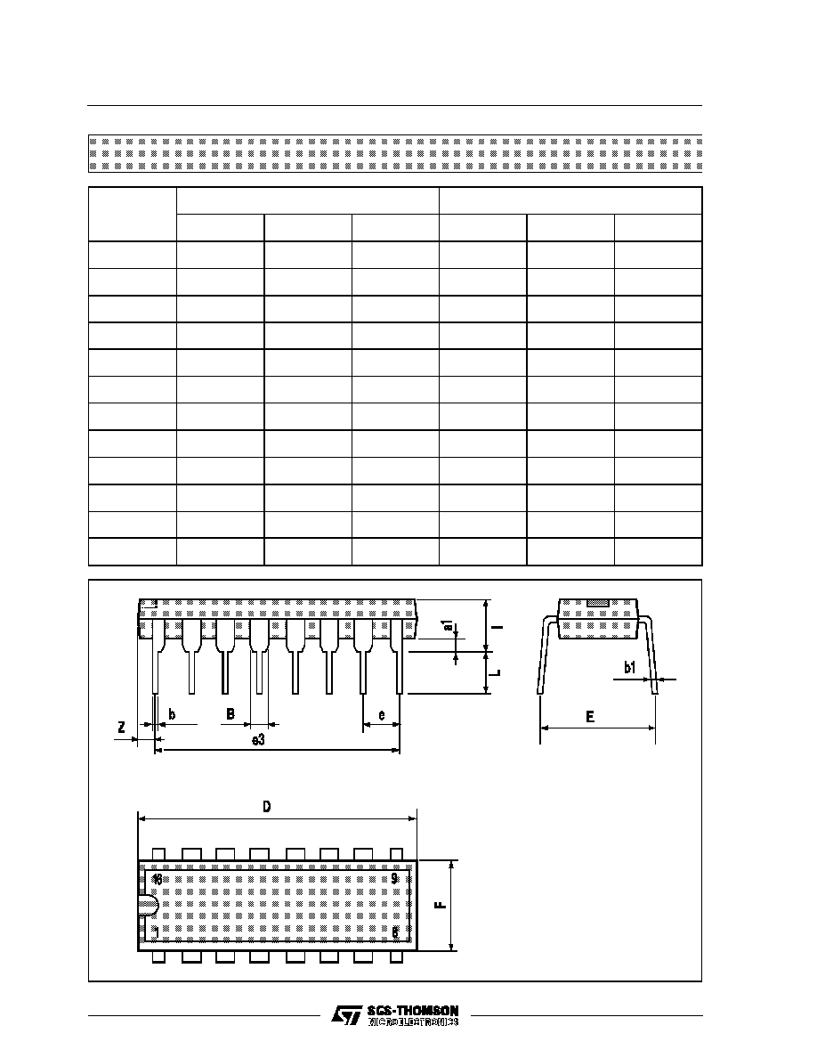
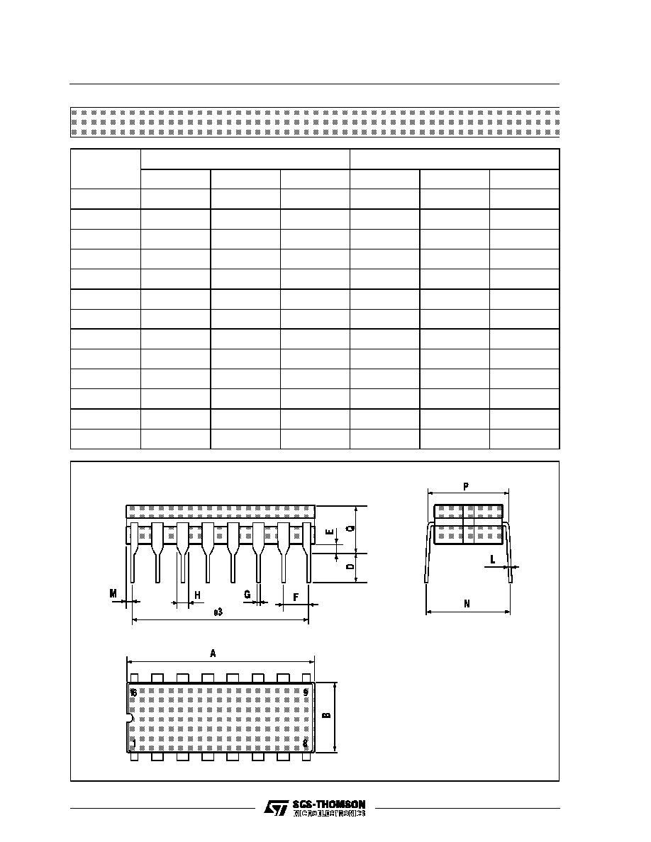
Plastic DIP16 (0.25) MECHANICAL DATA
DIM.
mm
inch
MIN.
TYP.
MAX.
MIN.
TYP.
MAX.
a1
0.51
0.020
B
0.77
1.65
0.030
0.065
b
0.5
0.020
b1
0.25
0.010
D
20
0.787
E
8.5
0.335
e
2.54
0.100
e3
17.78
0.700
F
7.1
0.280
I
5.1
0.201
L
3.3
0.130
Z
1.27
0.050
P001C
HCC/HCF4517B
9/12
Ceramic DIP16/1 MECHANICAL DATA
DIM.
mm
inch
MIN.
TYP.
MAX.
MIN.
TYP.
MAX.
A
20
0.787
B
7
0.276
D
3.3
0.130
E
0.38
0.015
e3
17.78
0.700
F
2.29
2.79
0.090
0.110
G
0.4
0.55
0.016
0.022
H
1.17
1.52
0.046
0.060
L
0.22
0.31
0.009
0.012
M
0.51
1.27
0.020
0.050
N
10.3
0.406
P
7.8
8.05
0.307
0.317
Q
5.08
0.200
P053D
HCC/HCF4517B
10/12
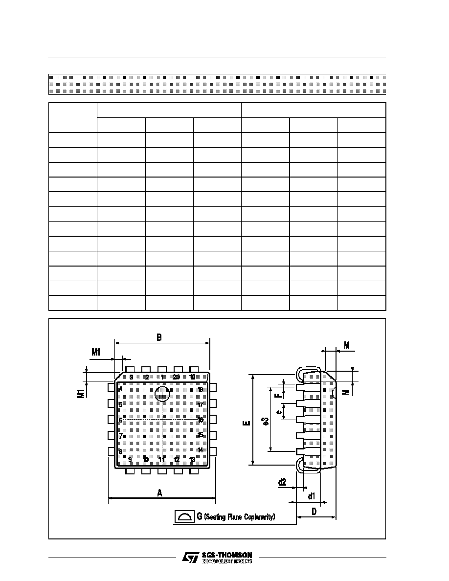
PLCC20 MECHANICAL DATA
DIM.
mm
inch
MIN.
TYP.
MAX.
MIN.
TYP.
MAX.
A
9.78
10.03
0.385
0.395
B
8.89
9.04
0.350
0.356
D
4.2
4.57
0.165
0.180
d1
2.54
0.100
d2
0.56
0.022
E
7.37
8.38
0.290
0.330
e
1.27
0.050
e3
5.08
0.200
F
0.38
0.015
G
0.101
0.004
M
1.27
0.050
M1
1.14
0.045
P027A
HCC/HCF4517B
11/12
Information furnished is believed to be accurate and reliable. However, SGS-THOMSON Microelectronics assumes no responsability for the
consequences of use of such information nor for any infringement of patents or other rights of third parties which may results from its use. No
license is granted by implication or otherwise under any patent or patent rights of SGS-THOMSON Microelectronics. Specifications mentioned
in this publication are subject to change without notice. This publication supersedes and replaces all information previously supplied.
SGS-THOMSON Microelectronics products are not authorized for use as critical components in life support devices or systems without express
written approval of SGS-THOMSON Microelectonics.
©
1994 SGS-THOMSON Microelectronics - All Rights Reserved
SGS-THOMSON Microelectronics GROUP OF COMPANIES
Australia - Brazil - France - Germany - Hong Kong - Italy - Japan - Korea - Malaysia - Malta - Morocco - The Netherlands -
Singapore - Spain - Sweden - Switzerland - Taiwan - Thailand - United Kingdom - U.S.A
HCC/HCF4517B
12/12