 | –≠–ª–µ–∫—Ç—Ä–æ–Ω–Ω—ã–π –∫–æ–º–ø–æ–Ω–µ–Ω—Ç: HCC4529BF | –°–∫–∞—á–∞—Ç—å:  PDF PDF  ZIP ZIP |

HCC4529B
HCF4529B
September 1988
ANALOG DATA SELECTOR
DUAL 4-CHANNEL OR SINGLE 8-CHANNEL
EY
(Plastic Package)
DESCRIPTION
ORDER CODES :
HCC4529BF
HCF4529BM1
HCF4529BEY
HCF4529BC1
F
(Ceramic Package)
M1
(Micro Package)
C1
(Chip Carrier)
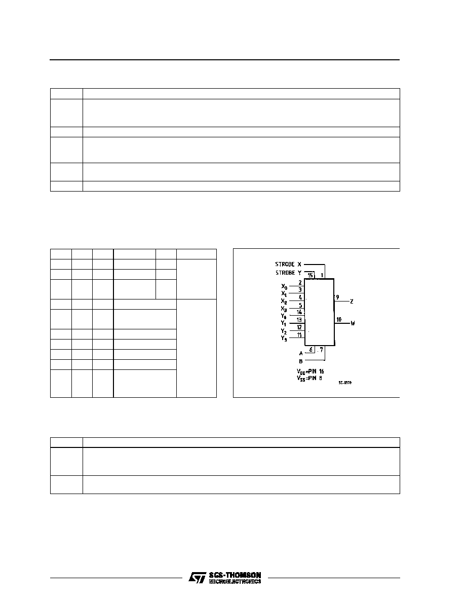
PIN CONNECTIONS
The HCC4529B (extended temperataure range)
and HCF4529b (intermediate temperature range)
are monolithic integrated circuits available in 16-
lead dual in line plastic or ceramic package and plas-
tic micropackage.
The HCC/HCF4529b is a DUAL 4-CHANNEL or 8-
CHANNEL device. One of the two possible function-
s can be selected by a proper input coding. For the
single 8-bit mode Z and W output must be tied
together.
HCC/HCF4529B is suitable for digital as well as
analogue applications, including 1 of 4 and 1 of 8
data selector functions. Dual binary to 1 of 4 or single
binary to 1 of 8 decoder applications can be im-
plemented because the device allow analogue and
bidirectional operation.
.
DATA PATHS ARE BIDIRECTIONAL
.
10 MHz OPERATION (typical)
.
3-STATE OUTPUTS
.
"ON" RESISTANCE 125 W TYPICAL @ 15V
.
SUPPLY VOLTAGE RANGE = 3Vdc TO 18Vdc
1/10
ABSOLUTE MAXIMUM RATING
Symbol
Parameter
Value
Unit
V
DD
*
Supply Voltage: HCC Types
HCF Types
-0.5 to +20
-0.5 to +18
V
V
V
i
Input Voltage
-0.5 to V
DD
+ 0.5
V
I
I
DC Input Current (any one input)
±
10
mA
P
tot
Total Power Dissipation (per package)
Dissipation per Output Transistor
for Top = Full Package Temperature Range
200
100
mW
mW
T
op
Operating Temperature: HCC Types
HCF Types
-55 to +125
-40 to +85
o
C
o
C
T
stg
Storage Temperature
-65 to +150
o
C
Stresses above those listed under "Absolute Maximum Ratings" may cause permanent damage to the device. This is a stress ratingonly and functional
operation of the device at these or any other conditions above those indicated in the operational sections of this specification is not implied. Exposure
to absolute maximum rating conditions for external periods may affect device reliability.
* All voltage values are referred to V
SS
pin voltage.
RECOMMENDED OPERATING CONDITIONS
Symbol
Parameter
Value
Unit
V
DD
Supply Voltage: HCC Types
HCF Types
3 to 18
3 to 15
V
V
V
I
Input Voltage
0 to V
DD
V
T
op
Operating Temperature: HCC Types
HCF Types
-55 to +125
-40 to +85
o
C
o
C
TRUTH TABLE
ST
X
ST
Y
B
A
Z
W
MODE
1
1
0
0
X0
Y0
Dual
4-Channel
Mode
2 Outputs
1
1
0
1
X1
Y1
1
1
1
0
X2
Y2
1
1
1
1
X3
Y3
1
0
0
0
X0
Single
8-Channel
Mode
1 Output
(Z and W
tied
together)
1
0
0
1
X1
1
0
1
0
X2
1
0
1
1
X3
0
1
0
0
Y0
0
1
0
1
Y1
0
1
1
0
Y2
0
1
1
1
Y3
0
0
X
X
High
Impedance
X = Don't care
FUNCTIONAL DIAGRAM
HCC/HCF4529B
2/10
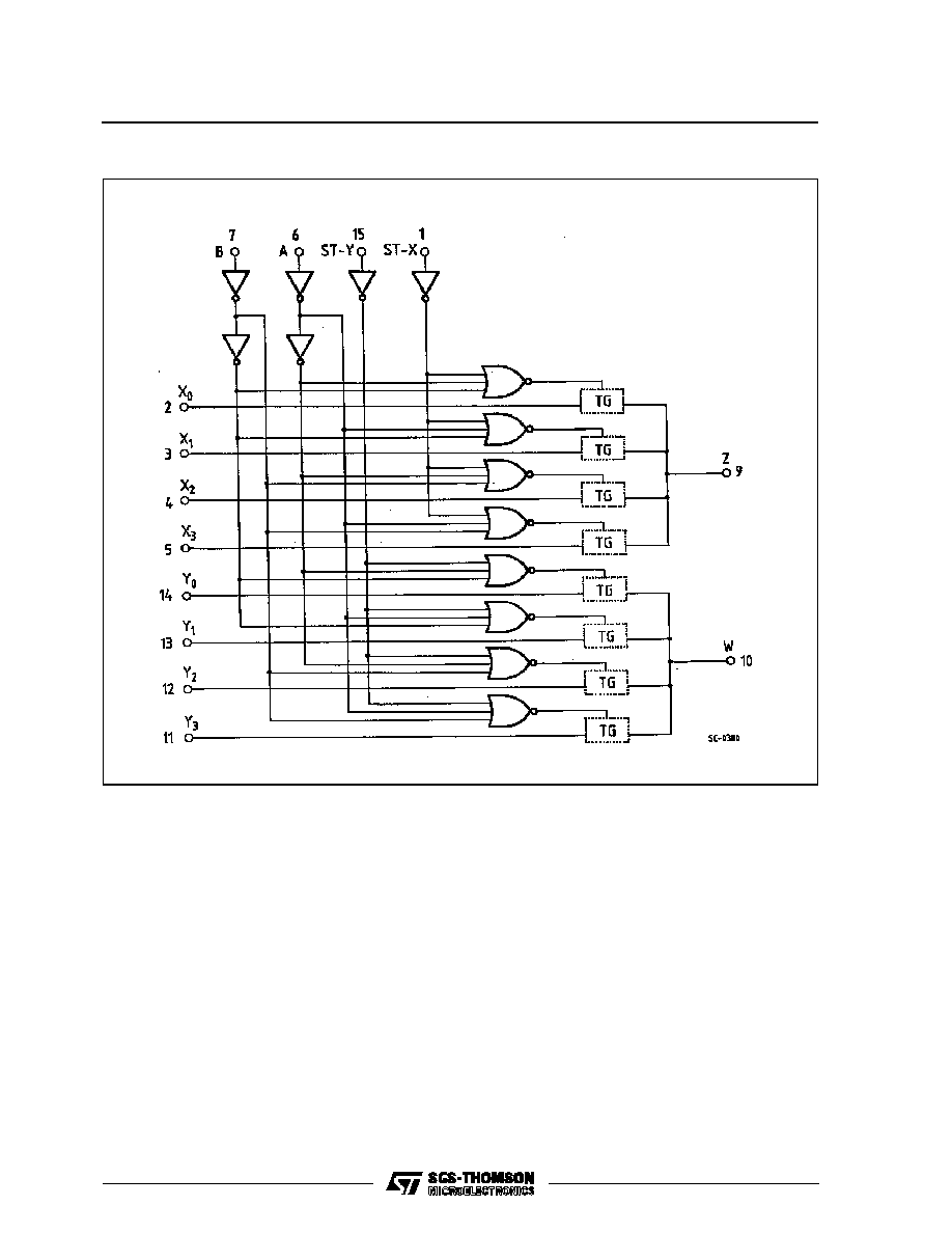
BLOCK DIAGRAM
HCC/HCF4529B
3/10

STATIC ELECTRICAL CHARACTERISTICS (over recommended operating conditions)
Symbol
Parameter
Test Conditios
Value
Unit
V
IS
(V)
V
SS
(V)
V
DD
(V)
T
LOW
*
25
o
C
T
HIGH
*
Min.
Max.
Min.
Typ.
Max.
Min.
Max.
I
L
Quiescent
Current
HCC
Types
5
5
0.04
5
150
µ
A
10
10
0.04
10
300
15
20
0.04
20
600
20
100
0.08
100
3000
HCF
Types
5
20
0.04
20
150
10
40
0.04
40
300
15
80
0.04
80
600
SWITCH
ON
Resistance
HCC
Types
0
V
I
V
DD
0
5
880
470
1050
1200
10
310
180
400
580
15
220
125
280
400
HCC
Types
0
V
I
V
DD
0
5
880
470
1050
1200
10
330
180
400
520
15
230
125
280
360
ON
Resistance
R
ON
(Between any 2
channels)
0
5
10
10
10
15
5
OFF
Channel
Leakage
Current
Any
Channel
OFF
HCC
Types
0
18
100
±
0.1
100
1000
nA
All Channel
OFF
(common
OUT/IN)
HCC
Types
0
18
100
±
0.1
100
1000
nA
Any
Channel
OFF
HCC
Types
0
15
300
±
0.1
300
1000
nA
All Channel
OFF
(common
OUT/IN)
HCC
Types
0
15
300
±
0.1
300
1000
nA
CONTROL (Address or Inhibit)
V
IL
Input Low
Voltage
= V
DD
thru
1K
R
L
=1K
to V
SS
I
IS
< 2
µ
A
(On All
OFF
Channels)
5
1.5
1.5
1.5
V
10
3
3
3
15
4
4
4
V
IH
Input High
Voltage
5
3.5
3.5
3.5
V
10
7
7
7
15
11
11
11
I
IH
, I
IL
Input
Leakage
Current
HCC
Types
V
I
= 0/18V
18
±
0.1
±
10
-3
±
0.1
±
1
µ
A
HCF
Types
V
I
= 0/15V
15
±
0.3
±
10
-3
±
0.3
±
1
C
I
Input Capacitance
Any Input
5
7.5
pF
* T
LOW
= -55
o
C for HCC device: -40
o
C for HCF device.
* T
HIGH
= +125
o
C for HCC device: +85
o
C for HCF device.
The Noise Margin for both "1" and "0" level is: 1V min. with V
DD
= 5 V, 2 V min. with V
DD
= 10 V, 2.5 V min. with V
DD
= 15 V
HCC/HCF4529B
4/10
DYNAMIC ELECTRICAL CHARACTERISTICS (T
amb
= 25
o
C, C
L
= 50 pF, R
L
= 200 K
,
typical temperature coefficent for all V
DD
values is 03 %/
o
C, all input rise and fall times= 20 ns)
Symbol
Parameter
Test Conditions
Value
Unit
V
SS
(V) V
DD
(V)
Min.
Typ.
Max.
t
PLH
t
PHL
V
in
to V
out
Propagation Delay Time
(C
L
= 50pF, R
L
= 1K
)
0
5
20
40
ns
10
10
20
15
8
15
t
PLH
t
PHL
Propagation Delay Time, Control to Output,
Vin = V
DD
or V
SS
(V
in
10 Vdc, C
L
= 50pF, R
L
= 1 K
)
0
5
200
400
ns
10
80
160
15
50
120
Crosstalk, Control to Output
(C
L
= 50pF, R
L
= 1 K
, R
out
= 10 K
)
0
5
5
mV
10
5
15
5
Maximum Control Input Pulse Frequency
(C
L
= 50pF, R
L
= 1 K
)
0
5
5
MHz
10
10
15
12
Sine Wave (Distortion) (V
in
= 1.77 Vdc RMS
Centred @ 0.0 Vdc, R
L
= 10 K
, f = 1 KHz)
-5
5
0.36
%
BW
Bandwidth (-3 dB) (V
in
= 1.77 Vdc RMS
Centred @ 0.0 Vdc)
(R
L
= 1K
)
(R
L
= 10K
)
(R
L
= 100K
)
(R
L
= 1M
)
-5
5
35
28
27
26
MHz
Feedthrough and Crosstalk
20
Log
10
V
out
V
in
= -
50
dB
(R
L
= 1K
)
(R
L
= 10K
)
(R
L
= 100K
)
(R
L
= 1M
)
-5
5
850
100
12
1.5
KHz
HCC/HCF4529B
5/10

Plastic DIP16 (0.25) MECHANICAL DATA
DIM.
mm
inch
MIN.
TYP.
MAX.
MIN.
TYP.
MAX.
a1
0.51
0.020
B
0.77
1.65
0.030
0.065
b
0.5
0.020
b1
0.25
0.010
D
20
0.787
E
8.5
0.335
e
2.54
0.100
e3
17.78
0.700
F
7.1
0.280
I
5.1
0.201
L
3.3
0.130
Z
1.27
0.050
P001C
HCC/HCF4529B
6/10

Ceramic DIP16/1 MECHANICAL DATA
DIM.
mm
inch
MIN.
TYP.
MAX.
MIN.
TYP.
MAX.
A
20
0.787
B
7
0.276
D
3.3
0.130
E
0.38
0.015
e3
17.78
0.700
F
2.29
2.79
0.090
0.110
G
0.4
0.55
0.016
0.022
H
1.17
1.52
0.046
0.060
L
0.22
0.31
0.009
0.012
M
0.51
1.27
0.020
0.050
N
10.3
0.406
P
7.8
8.05
0.307
0.317
Q
5.08
0.200
P053D
HCC/HCF4529B
7/10

SO16 (Narrow) MECHANICAL DATA
DIM.
mm
inch
MIN.
TYP.
MAX.
MIN.
TYP.
MAX.
A
1.75
0.068
a1
0.1
0.2
0.004
0.007
a2
1.65
0.064
b
0.35
0.46
0.013
0.018
b1
0.19
0.25
0.007
0.010
C
0.5
0.019
c1
45
∞
(typ.)
D
9.8
10
0.385
0.393
E
5.8
6.2
0.228
0.244
e
1.27
0.050
e3
8.89
0.350
F
3.8
4.0
0.149
0.157
G
4.6
5.3
0.181
0.208
L
0.5
1.27
0.019
0.050
M
0.62
0.024
S
8
∞
(max.)
P013H
HCC/HCF4529B
8/10
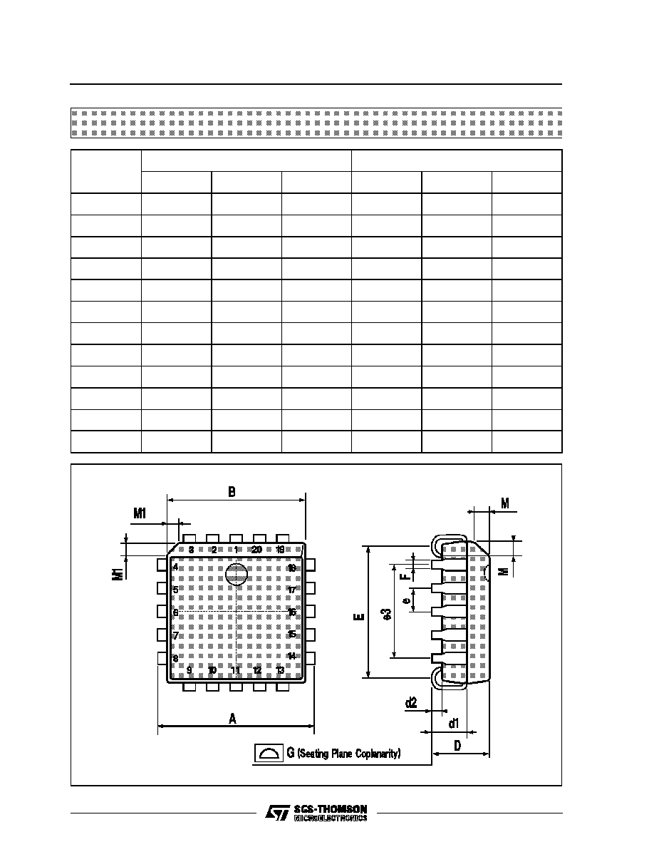
PLCC20 MECHANICAL DATA
DIM.
mm
inch
MIN.
TYP.
MAX.
MIN.
TYP.
MAX.
A
9.78
10.03
0.385
0.395
B
8.89
9.04
0.350
0.356
D
4.2
4.57
0.165
0.180
d1
2.54
0.100
d2
0.56
0.022
E
7.37
8.38
0.290
0.330
e
1.27
0.050
e3
5.08
0.200
F
0.38
0.015
G
0.101
0.004
M
1.27
0.050
M1
1.14
0.045
P027A
HCC/HCF4529B
9/10

Information furnished is believed to be accurate and reliable. However, SGS-THOMSON Microelectronics assumes no responsability for the
consequences of use of such information nor for any infringement of patents or other rights of third parties which may results from its use. No
license is granted by implication or otherwise under any patent or patent rights of SGS-THOMSON Microelectronics. Specifications mentioned
in this publication are subject to change without notice. This publication supersedes and replaces all information previously supplied.
SGS-THOMSON Microelectronics products are not authorized for use as critical components in life support devices or systems without express
written approval of SGS-THOMSON Microelectonics.
©
1994 SGS-THOMSON Microelectronics - All Rights Reserved
SGS-THOMSON Microelectronics GROUP OF COMPANIES
Australia - Brazil - France - Germany - Hong Kong - Italy - Japan - Korea - Malaysia - Malta - Morocco - The Netherlands -
Singapore - Spain - Sweden - Switzerland - Taiwan - Thailand - United Kingdom - U.S.A
HCC/HCF4529B
10/10