 | –≠–ª–µ–∫—Ç—Ä–æ–Ω–Ω—ã–π –∫–æ–º–ø–æ–Ω–µ–Ω—Ç: HCF40108B | –°–∫–∞—á–∞—Ç—å:  PDF PDF  ZIP ZIP |

HCC40108B
HCF40108B
September 1988
4 x 4 MULTIPORT REGISTER
EY
(Plastic Package)
DESCRIPTION
ORDER CODES :
HCC40108BF
HCF40108BM1
HCF40108BEY
HCF40108BC1
F
(Ceramic Package)
M1
(Micro Package)
C1
(Chip Carrier)
PIN CONNECTIONS
The HCC40108B (extended temperature range)
and HCF40108B (intermediate temperature range)
are monolithic integrated circuits, available in 24
lead dual in line plastic or ceramic packageand plas-
tic micropackage. The HCC/HCF40108B is a 4 X 4
multiport register containing four 4-bit register, write
address decoder, two separate read address
decoders, and two 3-state output buses. When the
ENABLE input is low, the corresponding output bus
is switched, independently of the clock, to a high im-
pedance state. The high impedance third state pro-
vides the outputs with the capability of being
connected to the bus lines in a bus organized sys-
tem without the need for interface or pull-up compo-
nents. When the WRITE ENABLE input is high, all
data input lines are latched on the positive transition
of the CLOCK and the data is entered into the word
selected by the write address lines. When WRITE
ENABLE is low, the CLOCK is inhibited and
.
FOUR 4-BIT REGISTERS
.
ONE INPUT AND TWO OUTPUT BUSES
.
UNLIMITED EXPANSION IN BIT AND WORD
DIRECTION
.
DATA LINES HAVE LATCHED INPUTS
.
3-STATE OUTPUTS
.
SEPARATE
CONTROL
OF
EACH
BUS,
ALLOWING SIMULTANEOUS INDEPENDET
READING AND ANY OF FOUR REGISTERS
ON BUS A AND BUS B AND INDEPENDENT
WRITING INTO ANY ANY OF THE FOUR REG-
ISTERS
.
40108B IS PIN COMPATIBLE WITH INDUSTRY
TYPE MC14580
.
STANDARDIZED, SYMMETRICAL OUTPUT
CHARACTERISTICS
.
QUIESCENT CURRENT SPECIFIED AT 20V
FOR HCC DEVICE
.
5V, 10V AND 15V PARAMETRIC RATINGS
.
INPUT CURRENTOF 100 nA AT 18V AND 25oC
FOR HCC DEVICE
.
100% TESTED FOR QUIESCENT CURRENT
.
MEETS ALL REQUIREMENTS OF JEDEC TEN-
TATIVE STANDARD No 13a, "STANDARD
SPECIFICATIONS FOR DESCRIPTION OF B
SERIES CMOS DEVICES"
no new data is netered. In either case, the contents
of any word may be accessed via the read address
lines independent of the state of the CLOCK input.
1/14
FUNCTIONAL DIAGRAM
LOGIC DIAGRAM
HCC/HCF40108
2/14
ABSOLUTE MAXIMUM RATING
Symbol
Parameter
Value
Unit
V
DD
*
Supply Voltage: HCC Types
HCF Types
-0.5 to +20
-0.5 to +18
V
V
V
i
Input Voltage
-0.5 to V
DD
+ 0.5
V
I
I
DC Input Current (any one input)
±
10
mA
P
tot
Total Power Dissipation (per package)
Dissipation per Output Transistor
for Top = Full Package Temperature Range
200
100
mW
mW
T
op
Operating Temperature: HCC Types
HCF Types
-55 to +125
-40 to +85
o
C
o
C
T
stg
Storage Temperature
-65 to +150
o
C
Stresses above those listed under "Absolute Maximum Ratings" may cause permanent damage to the device. This is a stress ratingonly and functional
operation of the device at these or any other conditions above those indicated in the operational sections of this specification is not implied. Exposure
to absolute maximum rating conditions for external periods may affect device reliability.
* All voltage values are referred to V
SS
pin voltage.
RECOMMENDED OPERATING CONDITIONS
Symbol
Parameter
Value
Unit
V
DD
Supply Voltage: HCC Types
HCF Types
3 to 18
3 to 15
V
V
V
I
Input Voltage
0 to V
DD
V
T
op
Operating Temperature: HCC Types
HCF Types
-55 to +125
-40 to +85
o
C
o
C
TRUTH TABLE
CLOCK
Write
Enable
Write
1
Write
2
Read
1A
Read
0A
Read
1B
Read
0B
Enable
A
Enable
B
D
n
Q
nA
Q
nB
1
S1
S2
S1
S2
S1
S2
1
1
1
1
1
1
S1
S2
S1
S2
S1
S2
1
0
0
0
0
X
X
X
X
X
X
X
X
0
X
Z
Z
Z
1
0
0
0
1
1
0
1
1
D
n
to
word 0
Word
1 Out
Word
2 Out
0
0
0
0
1
1
0
1
1
Word
0 not
altered
Word
1 Out
Word
2 Out
X
X
X
X
1
0
0
1
1
X
X
Word
2 Out
Word
1 Out
X
X
X
X
X
X
X
1
1
X
NC
NC
1 = HIGH LEVEL, 0 = LOW LEVEL, X = DON'T CARE, Z = HIGH IMPEDANCE
S1 and S2 refer to input strates of either 1 or 0
HCC/HCF40108
3/14
SCHEMATIC DIAGRAM
HCC/HCF40108
4/14
STATIC ELECTRICAL CHARACTERISTICS (over recommended operating conditions)
Symbol
Parameter
Test Conditios
Value
Unit
V
I
(V)
V
O
(V)
|I
O
|
(
µ
A)
V
DD
(V)
T
LOW
*
25
o
C
T
HIGH
*
Min.
Max.
Min.
Typ.
Max.
Min.
Max.
I
L
Quiescent
Current
HCC
Types
0/5
5
5
0.04
5
150
µ
A
0/10
10
10
0.04
10
300
0/15
15
20
0.04
20
600
0/20
20
100
0.08
100
3000
HCF
Types
0/5
5
20
0.04
20
150
0/10
10
40
0.04
40
300
0/15
15
80
0.04
80
600
V
OH
Output High
Voltage
0/5
< 1
5
4.95
4.95
4.95
V
0/10
< 1
10
9.95
9.95
9.95
0/15
< 1
15
14.95
14.95
14.95
V
OL
Output Low
Voltage
5/0
< 1
5
0.05
0.05
0.05
V
10/0
< 1
10
0.05
0.05
0.05
15/0
< 1
15
0.05
0.05
0.05
V
IH
Input High
Voltage
0.5/4.5
< 1
5
3.5
3.5
3.5
V
1/9
< 1
10
7
7
7
1.5/13.5
< 1
15
11
11
11
V
IL
Input Low
Voltage
4.5/0.5
< 1
5
1.5
1.5
1.5
V
9/1
< 1
10
3
3
3
13.5/1.5
< 1
15
4
4
4
I
OH
Output
Drive
Current
HCC
Types
0/5
2.5
5
-2
-1.6
-3.2
-1.15
mA
0/5
4.6
5
-0.64
-0.51
-1
-0.36
0/10
9.5
10
-1.6
-1.3
-2.6
-0.9
0/15
13.5
15
-4.2
-3.4
-6.8
-2.4
HCF
Types
0/5
2.5
5
-1.53
-1.36
-3.2
-1.1
0/5
4.6
5
-0.52
-0.44
-1
-0.36
0/10
9.5
10
-1.3
-1.1
-2.6
-0.9
0/15
13.5
15
-3.6
-3.0
-6.8
-2.4
I
OL
Output
Sink
Current
HCC
Types
0/5
0.4
5
0.64
0.51
1
0.36
mA
0/10
0.5
10
1.6
1.3
2.6
0.9
0/15
1.5
15
4.2
3.4
6.8
2.4
HCF
Types
0/5
0.4
5
0.52
0.44
1
0.36
0/10
0.5
10
1.3
1.1
2.6
0.9
0/15
1.5
15
3.6
3.0
6.8
2.4
I
IH
, I
IL
Input
Leakage
Current
HCC
Types
0/18
Any Input
18
±
0.1
±
10
-5
±
0.1
±
1
µ
A
HCF
Types
0/15
15
±
0.3
±
10
-5
±
0.3
±
1
I
OH
, I
OL
**
3-Sate
Output
Leakage
Current
HCC
Types
0/18
0/18
18
±
0.4
±
10
-4
±
0.4
±
12
µ
A
HCF
Types
0/15
0/15
15
±
1.0
±
10
-4
±
1.0
±
7.5
C
I
Input Capacitance
Any Input
5
7.5
pF
* T
LOW
= -55
o
C for HCC device: -40
o
C for HCF device.
* T
HIGH
= +125
o
C for HCC device: +85
o
C for HCF device.
The Noise Margin for both "1" and "0" level is: 1V min. with V
DD
= 5 V, 2 V min. with V
DD
= 10 V, 2.5 V min. with V
DD
= 15 V
** Forced output disable
HCC/HCF40108
5/14
DYNAMIC ELECTRICAL CHARACTERISTICS (T
amb
= 25
o
C, C
L
= 50 pF, R
L
= 200 K
,
typical temperature coefficent for all V
DD
values is 03 %/
o
C, all input rise and fall times= 20 ns)
Symbol
Parameter
Test Conditions
Value
Unit
V
DD
(V)
Min.
Typ.
Max.
t
PLH
t
PHL
Propagation Delay Time
Clock or Write Enable to Q
5
360
720
ns
10
140
280
15
100
200
Propagation Delay Time
Read or Write Address to Q
5
300
600
10
120
240
15
85
170
t
PZH
t
PHZ
3-State Disable Delay Time
5
100
200
ns
10
50
100
15
40
80
t
PZL
t
PLZ
3-State Display Delay Time
5
130
260
ns
10
60
120
15
50
100
t
TLH
t
THL
Output Transition Time
5
100
200
ns
10
50
100
15
40
80
t
setup
Setup Time
Data to Clock t
s(D)
5
0
-95
ns
10
0
-35
15
0
-20
Setup Time
Write Enable to Clock t
s(WE)
5
250
125
10
100
50
15
70
35
Setup Time
Write Address to Clock t
s(WA)
5
250
125
10
100
50
15
70
35
t
r
, t
s
Clock Rise and Fall Time
5
15
µ
s
10
5
15
5
t
hold
Hold Time
Data to Clock t
s(D)
5
220
110
ns
10
100
50
15
80
40
Hold Time
Write Enable to Clock t
s(WE)
5
270
135
10
130
65
15
80
40
Hold Time
Write Address to Clock t
s(WA)
5
330
165
10
140
70
15
90
45
t
W
Clock Pulse Width
Clock or Write Enable t
W(CL)
5
350
175
ns
10
130
65
15
90
45
Clock Pulse Width
Write Address t
W(WA)
5
300
150
10
150
75
15
90
45
f
CL
Maximum Clock Input Frequency
5
1.5
3
MHz
10
3.5
7
15
4.5
9
HCC/HCF40108
6/14

Output Low (sink) Current Characteristics
Typical Propagation Delay Time vs Load Capa-
citance (CL or WE to Q)
Typical Dynamic Power Dissipation vs Input Fre-
quency
Output High (source) Current Characteristics
Typical Transition Time vs Load Capacitance
HCC/HCF40108
7/14
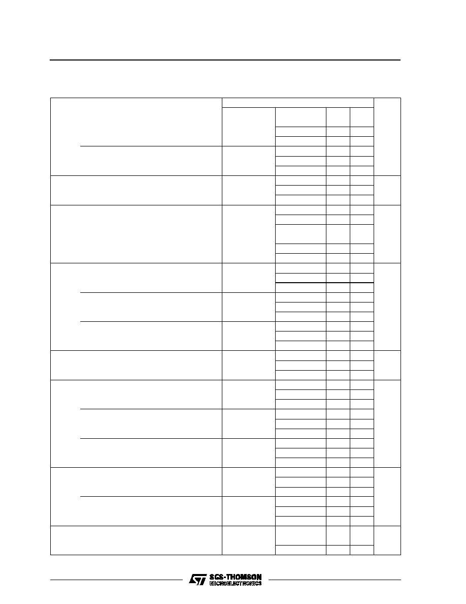
TIMING DIAGRAM
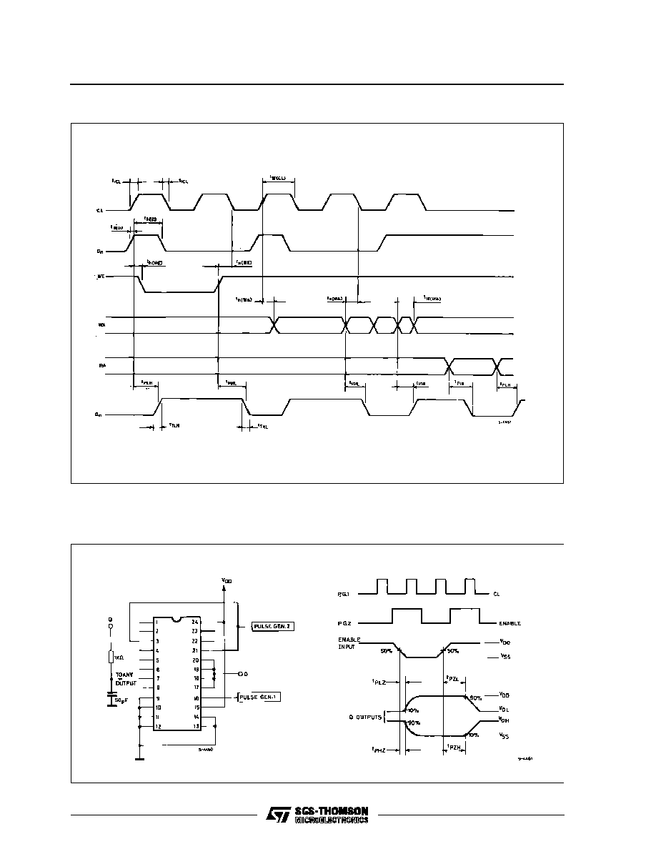
TEST CIRCUITS
Output Enable Delay Times and Waveforms
HCC/HCF40108
8/14
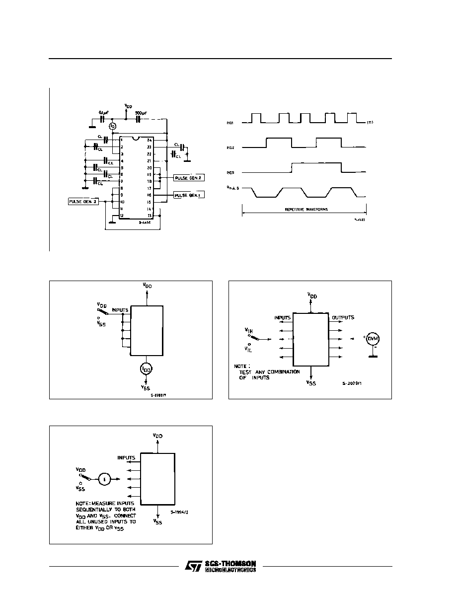
Quiescent Device Current.
Noise Immunity.
Input Leakage Current.
Power Dissipation and Waveforms
HCC/HCF40108
9/14
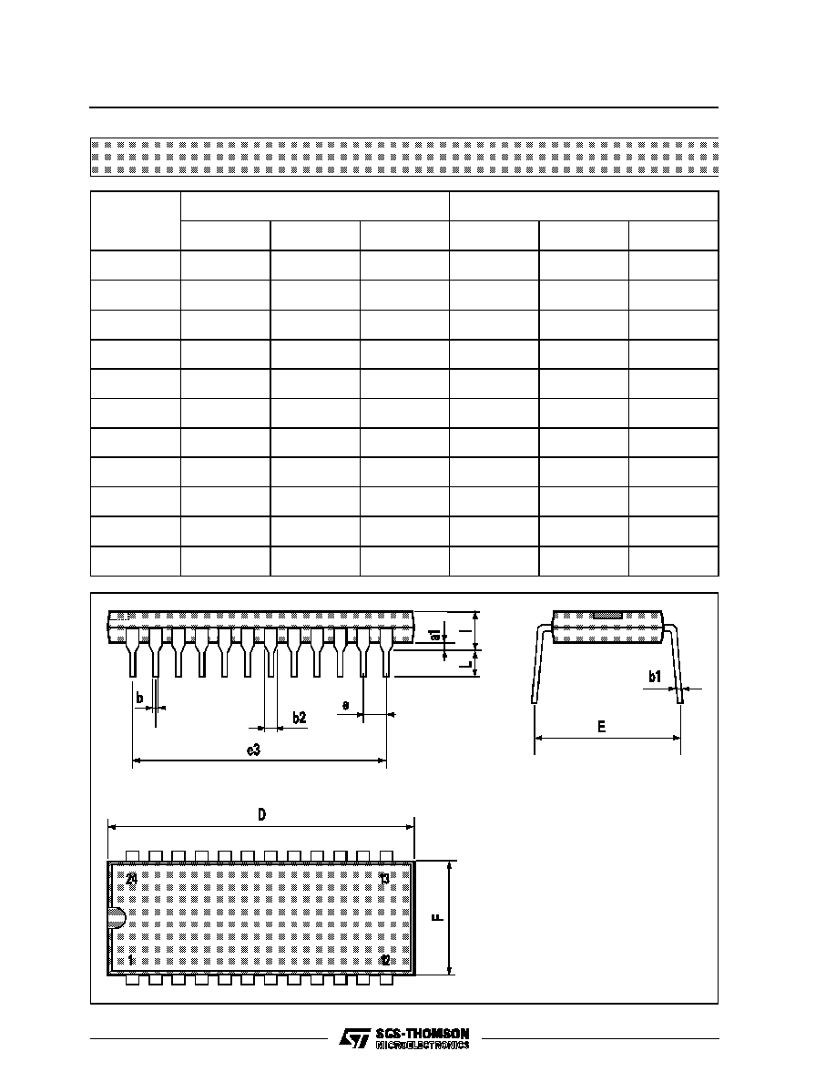
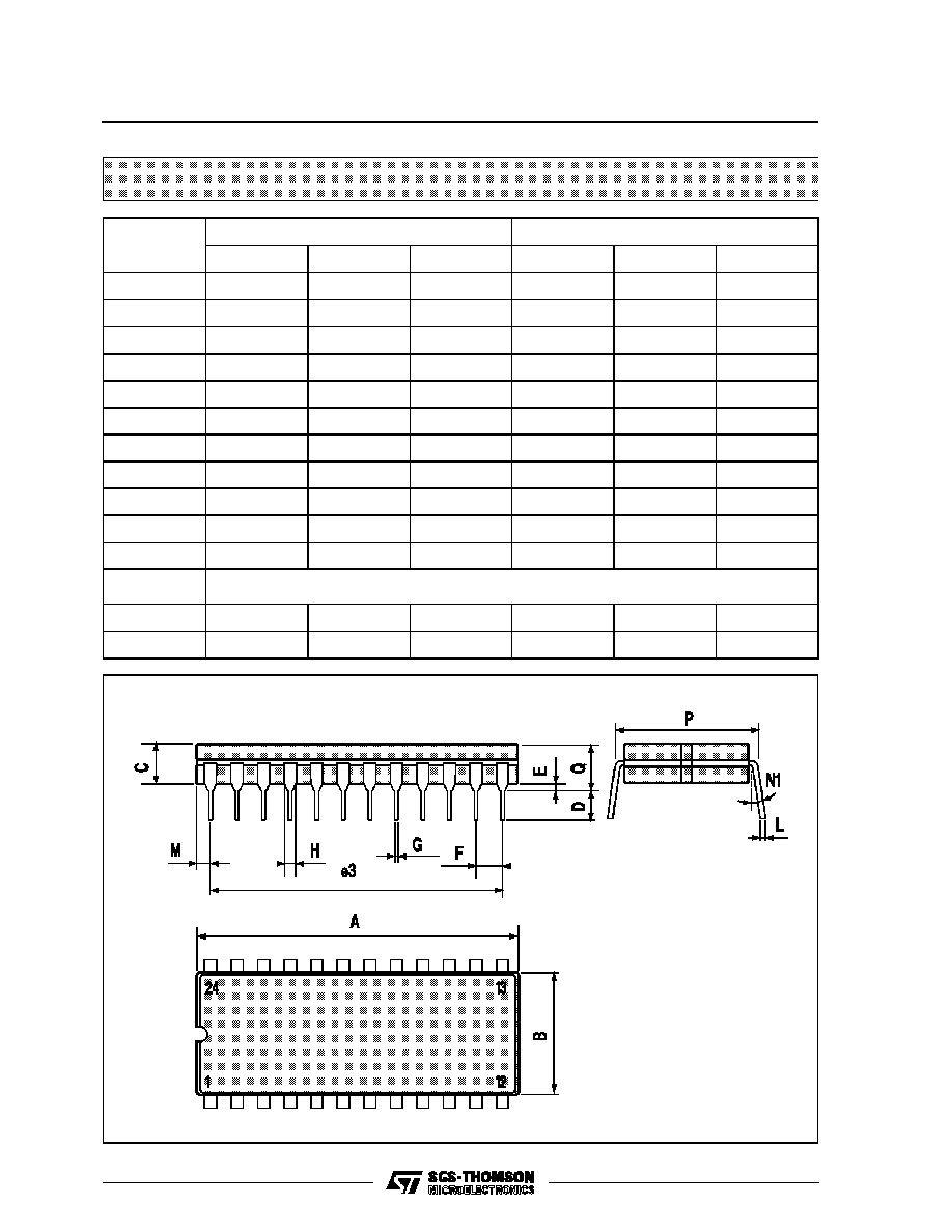
Plastic DIP24 (0.25) MECHANICAL DATA
DIM.
mm
inch
MIN.
TYP.
MAX.
MIN.
TYP.
MAX.
a1
0.63
0.025
b
0.45
0.018
b1
0.23
0.31
0.009
0.012
b2
1.27
0.050
D
32.2
1.268
E
15.2
16.68
0.598
0.657
e
2.54
0.100
e3
27.94
1.100
F
14.1
0.555
I
4.445
0.175
L
3.3
0.130
P043A
HCC/HCF40108
10/14
Ceramic DIP24 MECHANICAL DATA
DIM.
mm
inch
MIN.
TYP.
MAX.
MIN.
TYP.
MAX.
A
32.3
1.272
B
13.05
13.36
0.514
0.526
C
3.9
5.08
0.154
0.200
D
3
0.118
E
0.5
1.78
0.020
0.070
e3
27.94
1.100
F
2.29
2.79
0.090
0.110
G
0.4
0.55
0.016
0.022
I
1.17
1.52
0.046
0.060
L
0.22
0.31
0.009
0.012
M
1.52
2.49
0.060
0.098
N1
4
∞
(min.), 15
∞
(max.)
P
15.4
15.8
0.606
0.622
Q
5.71
0.225
P058C
HCC/HCF40108
11/14
SO24 MECHANICAL DATA
DIM.
mm
inch
MIN.
TYP.
MAX.
MIN.
TYP.
MAX.
A
2.65
0.104
a1
0.10
0.20
0.004
0.007
a2
2.45
0.096
b
0.35
0.49
0.013
0.019
b1
0.23
0.32
0.009
0.012
C
0.50
0.020
c1
45
∞
(typ.)
D
15.20
15.60
0.598
0.614
E
10.00
10.65
0.393
0.420
e
1.27
0.05
e3
13.97
0.55
F
7.40
7.60
0.291
0.299
L
0.50
1.27
0.19
0.050
S
8
∞
(max.)
F
C
L
E
a1
b1
A
e
D
e3
b
24
13
1
12
c1
s
a2
HCC/HCF40108
12/14
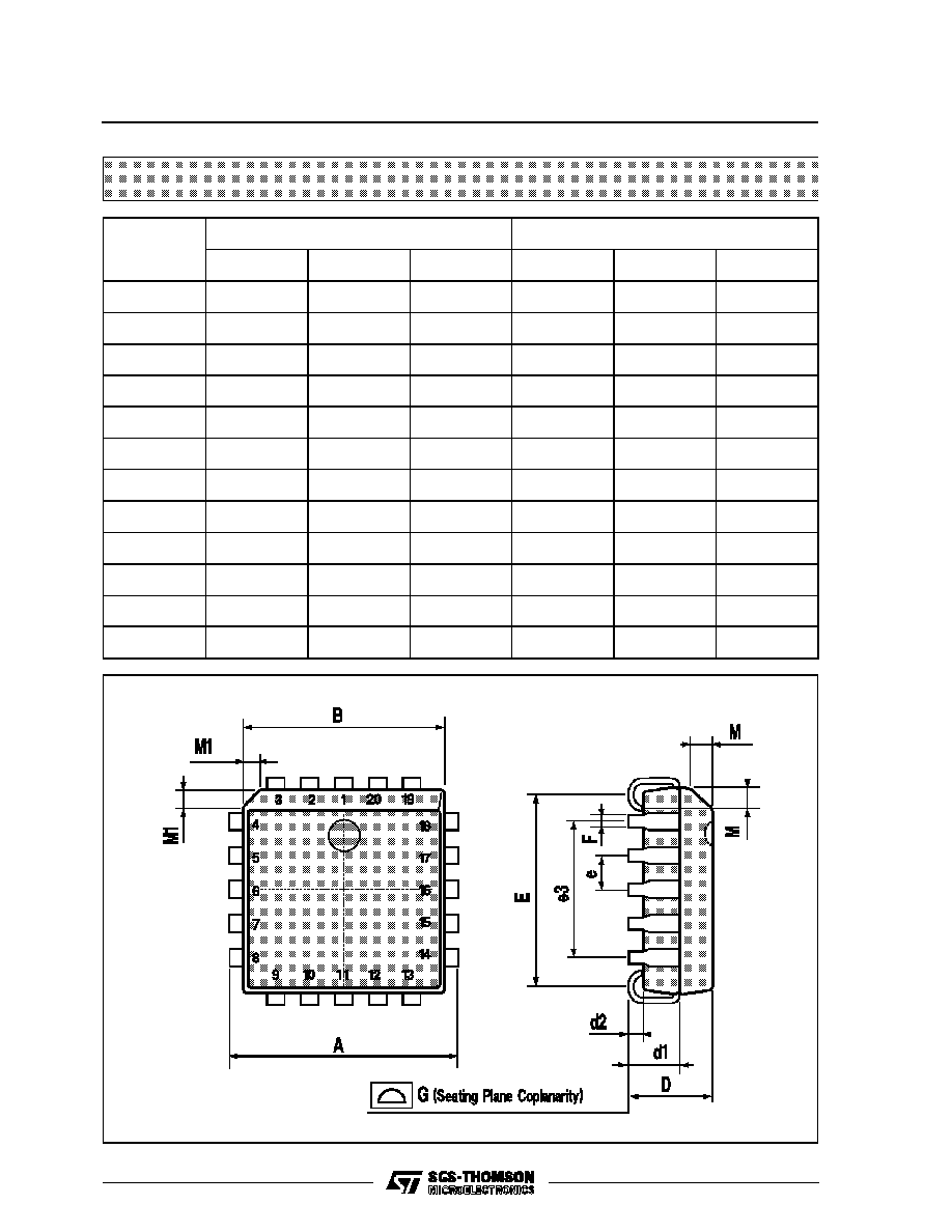
PLCC20 MECHANICAL DATA
DIM.
mm
inch
MIN.
TYP.
MAX.
MIN.
TYP.
MAX.
A
9.78
10.03
0.385
0.395
B
8.89
9.04
0.350
0.356
D
4.2
4.57
0.165
0.180
d1
2.54
0.100
d2
0.56
0.022
E
7.37
8.38
0.290
0.330
e
1.27
0.050
e3
5.08
0.200
F
0.38
0.015
G
0.101
0.004
M
1.27
0.050
M1
1.14
0.045
P027A
HCC/HCF40108
13/14

Information furnished is believed to be accurate and reliable. However, SGS-THOMSON Microelectronics assumes no responsability for the
consequences of use of such information nor for any infringement of patents or other rights of third parties which may results from its use. No
license is granted by implication or otherwise under any patent or patent rights of SGS-THOMSON Microelectronics. Specifications mentioned
in this publication are subject to change without notice. This publication supersedes and replaces all information previously supplied.
SGS-THOMSON Microelectronics products are not authorized for use as critical components in life support devices or systems without express
written approval of SGS-THOMSON Microelectonics.
©
1994 SGS-THOMSON Microelectronics - All Rights Reserved
SGS-THOMSON Microelectronics GROUP OF COMPANIES
Australia - Brazil - France - Germany - Hong Kong - Italy - Japan - Korea - Malaysia - Malta - Morocco - The Netherlands -
Singapore - Spain - Sweden - Switzerland - Taiwan - Thailand - United Kingdom - U.S.A
HCC/HCF40108
14/14