HCC40110B
HCF40110B
September 1988
DECADE UP-DOWN COUNTER/DECODER/LATCH/DRIVER
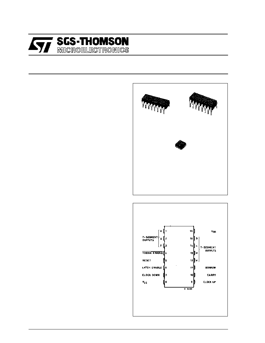
EY
(Plastic Package)
DESCRIPTION
ORDER CODES :
HCC40110BF
HCF40110BEY
HCF40110BC1
F
(Ceramic Package)
C1
(Chip Carrier)
PIN CONNECTIONS
The HCC 40110B (extended temperature range)
and HCF 40110B (intermediate temperature range)
are monolithic integrated circuits, available in 16-
lead dual in-line plastic or ceramic package. The
HCC/HCF 40110B is a dual-clocked up/down
counter with a special preconditioning circuit that
allows the counter to be clocked, via positive going
inputs, up or down regardless of that state or timing
(within 100 ns typ.) of the other clock line. The clock
signal is fed into the control logic and Johnson
counter after is preconditioned. The outputs of the
Johnson counter (which include antilock gating to
avoid being locked at an illegal state) are fed into a
latch. This data can be fed directly to the decoder
through the latch or can be strobed to hold a particu-
lar count while the Johnson counter continues to be
clocked. The decoder feeds a seven-segment bipo-
lar output driver which can source up to 25 mA to
drive LEDs and other displays such as low-voltage
fluorescent and incandescent lamps. A short dura-
tion negative-going pulse appears on the BORROW
output when the count changes from 0 to 9 or the
CARRY output when the count changes from 9 to
0. At the other times the BORROW and CARRY out-
put are a logic 1. The CARRY and BORROW out-
puts can be tied directly to the clock-up and
clock-down lines respectively of another HCC/HCF
40110B for easy cascading of several counters.
.
SEPARATE CLOCK-UP AND CLOCK-DOWN
LINES
.
CAPABLE OF DRIVING COMMON CATHODE
LEDS AND OTHER DISPLAYS DIRECTLY
.
ALLOWS CASCADING WITHOUT ANY EX-
TERNAL CIRCUITRY
.
MAXIMUM INPUT CURRENT OF 1
µ
A AT 18 V
(full package-temperature range)
.
QUIESCENT CURRENT AT 20 V FOR HCC DE-
VICE
.
5 V, 10 V AND 15 V PARAMETRIC RATINGS
.
INPUT CURRENT OF 100 nA AT 18 V AND
25
∞
C FOR HCC DEVICE
.
100 % TESTED FOR QUIESCENT CURRENT
.
MEETS ALL REQUIREMENTS OF JEDEC TEN-
TATIVE STANDARD No. 13 A, "STANDARD
SPECIFICATIONS FOR DESCRIPTION OF "B"
SERIES CMOS DEVICES"
1/11

ABSOLUTE MAXIMUM RATING
Symbol
Parameter
Value
Unit
V
DD
*
Supply Voltage: HCC Types
HCF Types
-0.5 to +20
-0.5 to +18
V
V
V
i
Input Voltage
-0.5 to V
DD
+ 0.5
V
I
I
DC Input Current (any one input)
±
10
mA
P
tot
Total Power Dissipation (per package)
Dissipation per Output Transistor
for Top = Full Package Temperature Range
200
100
mW
mW
T
op
Operating Temperature: HCC Types
HCF Types
-55 to +125
-40 to +85
o
C
o
C
T
stg
Storage Temperature
-65 to +150
o
C
Stresses above those listed under "Absolute Maximum Ratings" may cause permanent damage to the device. This is a stress ratingonly and functional
operation of the device at these or any other conditions above those indicated in the operational sections of this specification is not implied. Exposure
to absolute maximum rating conditions for external periods may affect device reliability.
* All voltage values are referred to V
SS
pin voltage.
RECOMMENDED OPERATING CONDITIONS
Symbol
Parameter
Value
Unit
V
DD
Supply Voltage: HCC Types
HCF Types
3 to 18
3 to 15
V
V
V
I
Input Voltage
0 to V
DD
V
T
op
Operating Temperature: HCC Types
HCF Types
-55 to +125
-40 to +85
o
C
o
C
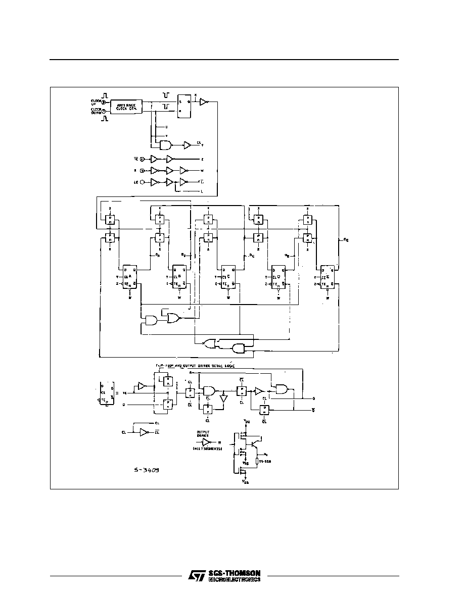
FUNCTIONAL DIAGRAM
HCC/HCF40110B
2/11

LOGIC DIAGRAM (continued)
DISPLAY SEGMENTS
Ouptut Low (sink) Current Characterisitcs.
TRUTH TABLE
CLOCK UP*
CLOCK
DOWN*
LATCH
ENABLE
TOGGLE
ENABLE
RESET
COUNTER
DISPLAY
X
0
0
0
Increments by 1
Follows Counter
X
0
0
0
Decrement by 1
Follows Counter
X
X
0
No Change
No Change
X
X
X
X
1
Goes to 00000
Follows Counter
(Display = 0 )
X
X
X
1
0
Inhibited
Remains Fixed
X
1
0
0
Increments by 1
Remains Fixed
X
1
0
0
Decrement by 1
Remains Fixed
x = Don't care 1 = High State 2 = Low State
* Typically 100 ns between clock-up and clock-down positive transitions are required to ensure proper counting
HCC/HCF40110B
4/11
STATIC ELECTRICAL CHARACTERISTICS (over recommended operating conditions)
Symbol
Parameter
Test Conditios
Value
Unit
V
I
(V)
V
O
(V)
|I
O
|
(
µ
A)
V
DD
(V)
T
LOW
*
25
o
C
T
HIGH
*
Min.
Max.
Min.
Typ.
Max.
Min.
Max.
I
L
Quiescent
Current
HCC
Types
0/5
5
5
0.04
5
150
µ
A
0/10
10
10
0.04
10
300
0/15
15
15
0.04
20
600
0/20
20
20
0.48
100
3000
HCF
Types
0/5
5
5
0.04
20
150
0/10
10
10
0.04
40
300
0/15
15
15
0.04
80
600
V
OH
Output High
Voltage
0/5
5
4.95
V
0/10
10
9.55
0/15
15
14.55
V
OL
Output Low
Voltage
5/0
5
0.05
0
0.05
0.05
V
10/0
10
0.05
0
0.05
0.05
15/0
15
0.05
0
0.05
0.05
V
IH
Input High
Voltage
0.5/3.8
5
3.5
3.5
3.5
V
1/8.8
10
7
7
7
1.5/3.8
15
11
11
11
V
IL
Input Low
Voltage
0.5/3.8
5
1.5
1.5
1.5
V
1/8.8
10
3
3
3
1.5/3.8
15
4
4
4
V
OL
Output Drive
Voltage
(for HCC/HCF)
0
5
4.55
V
10
5
4.13
25
5
3.64
0
10
9.55
10
10
9.25
25
10
8.85
0
15
14.55
10
15
14.21
25
15
13.9
I
OL
Output
Sink
Current
HCC
Types
0/5
0.4
5
0.64
0.51
1
0.36
mA
0/10
0.5
10
1.6
1.3
2.6
0.9
0/15
1.5
15
4.2
3.4
6.8
2.4
HCF
Types
0/5
0.4
5
0.52
0.44
1
0.36
0/10
0.5
10
1.3
1.1
2.6
0.9
0/15
1.5
15
3.6
3.0
6.8
2.4
I
IH
, I
IL
Input
Leakage
Current
HCC
Types
0/18
Any Input
18
±
0.1
±
10
-5
±
0.1
±
1
µ
A
HCF
Types
0/15
15
±
0.3
±
10
-5
±
0.3
±
1
C
I
Input Capacitance
Any Input
5
7.5
pF
* T
LOW
= -55
o
C for HCC device: -40
o
C for HCF device.
* T
HIGH
= +125
o
C for HCC device: +85
o
C for HCF device.
The Noise Margin for both "1" and "0" level is: 1V min. with V
DD
= 5 V, 2 V min. with V
DD
= 10 V, 2.5 V min. with V
DD
= 15 V
HCC/HCF40110
5/11