
HCC/HCF40160B-40161B
HCC/HCF40162B-40163B
September 1988
SYNCHRONOUS PROGRAMMABLE 4-BIT COUNTERS
EY
(Plastic Package)
DESCRIPTION
ORDER CODES :
HCC40XXXBF
HCF40XXXBEY
HCF40XXXBC1
F
(Ceramic Package)
C1
(Chip Carrier)
PIN CONNECTIONS
The HCC40160B, 40161B, 40162B, 40163B (ex-
tended temperature range) and HCF40160B,
40161B, 40162B, 40163B (intermediate tempera-
ture range) are monolithic integrated circuits, avail-
able in 16-lead dual in line plastic or ceramic
package and plastic micropackage.
HCC/HCF40160B, 40161B, 40162B and 40163B
are 4-bit synchronous programmable counters. The
CLEAR function of the HCC/HCF40162B and
40163B is synchronous and a low on the at the clear
CLEAR input sets all four outputs low on the next
positive CLOCK edge. The CLEAR function of the
HCC/HCF40160B and 40161B is asynchronous
and a low level at the CLEAR input sets all four out-
puts low regardless of the state of the CLOCK,
LOAD or ENABLE inputs. A low level at the LOAD
input disables the counter and causes the output to
agree with the set-up data after the next CLOCK
pulse regardless of the conditions of the ENABLE in-
.
INTERNAL LOOK-AHEAD FOR FAST COUNT-
ING
.
CARRY OUTPUT FOR CASCADING
.
SYNCHRONOUSLY PROGRAMMABLE
.
LOW-POWER TTL COMPATIBILITY
.
STANDARDIZED
SYMMETRICAL
OUTPUT
CHARACTERISTICS
.
QUIESCENT CURRENT SPECIFIED AT 20V
FOR HCC DEVICE
.
5V, 10V AND 15V PARAMETRIC RATINGS
.
INPUT CURRENT OF 100nA AT 18V AND 25oC
FOR HCC DEVICE
.
100% TESTED FOR QUIESCENT CURRENT
.
MEETS ALL REQUIREMENTS OF JEDEC TEN-
TATIVE STANDARD N. 13A, " STANDARD
SPECIFICATIONS FOR DESCRIPTION OF B
SERIES CMOS DEVICES "
40160B - DECADE WITH ASYNCHRONOUS
CLEAR
40161B - BINARY WITH ASYNCHRONOUS
CLEAR
40162B - DECADE WITH SYNCHRONOUS
CLEAR
40163B - BINARY WITH SYNCHRONOUS
CLEAR
M1
(Micro Package)
1/15

ABSOLUTE MAXIMUM RATING
Symbol
Parameter
Value
Unit
V
DD
*
Supply Voltage: HCC Types
HCF Types
-0.5 to +20
-0.5 to +18
V
V
V
i
Input Voltage
-0.5 to V
DD
+ 0.5
V
I
I
DC Input Current (any one input)
±
10
mA
P
tot
Total Power Dissipation (per package)
Dissipation per Output Transistor
for Top = Full Package Temperature Range
200
100
mW
mW
T
op
Operating Temperature: HCC Types
HCF Types
-55 to +125
-40 to +85
o
C
o
C
T
stg
Storage Temperature
-65 to +150
o
C
Stresses above those listed under "Absolute Maximum Ratings" may cause permanent damage to the device. This is a stress ratingonly and functional
operation of the device at these or any other conditions above those indicated in the operational sections of this specification is not implied. Exposure
to absolute maximum rating conditions for external periods may affect device reliability.
* All voltage values are referred to V
SS
pin voltage.
cascading counter for n-bit synchronour application
without additional gating. Instrumental in accom-
plishing this function are two count-enable input
and a carry output (COUT). Counting is enable
when both PE and TE inputs are high. The TE input
is fed forward to enable COUT. This enable output
produces a positive output pulse with a duration ap-
proximately equal to the positive portion of the Q1
output. This positive overflow carry pulse can be
used to enable successive cascaded stages. Logic
transitions at the PE or TE inputs may occur when
the clock is either high or low.
RECOMMENDED OPERATING CONDITIONS
Symbol
Parameter
Value
Unit
V
DD
Supply Voltage: HCC Types
HCF Types
3 to 18
3 to 15
V
V
V
I
Input Voltage
0 to V
DD
V
T
op
Operating Temperature: HCC Types
HCF Types
-55 to +125
-40 to +85
o
C
o
C
TRUTH TABLE
Clock
CLR
LOAD
PE
TE
Operation
1
0
X
X
Preset
1
1
0
X
NC
1
1
X
0
NC
1
1
1
1
Count
X
0
X
X
X
Reset (HCC/HCF40160B, HCC/HCF40161B)
0
X
X
X
Reset (HCC/HCF40162B, HCC/HCF40163B)
1
X
X
X
NC (HCC/HCF40162B, HCC/HCF40163B)
1 = HIGH LEVEL, 0 = LOW LEVEL, X = DON'T CARE, NC = NO CHANGE
HCC/HCF40160B-40161B-40162-40163
2/15

LOGIC DIAGRAMS
HCC40161B/HCC40163B
HCC40160B/HCC40162B
HCC/HCF40160B-40161B-40162B-40163B
3/15

TIMING DIAGRAMS
HCC40161B/HCC40163B
HCC40160B/HCC40162B
HCC/HCF40160B-40161B-40162-40163
4/15

STATIC ELECTRICAL CHARACTERISTICS (over recommended operating conditions)
Symbol
Parameter
Test Conditios
Value
Unit
V
I
(V)
V
O
(V)
|I
O
|
(
µ
A)
V
DD
(V)
T
LOW
*
25
o
C
T
HIGH
*
Min.
Max.
Min.
Typ.
Max.
Min.
Max.
I
L
Quiescent
Current
HCC
Types
0/5
5
5
0.04
5
150
µ
A
0/10
10
10
0.04
10
300
0/15
15
20
0.04
20
600
0/20
20
100
0.08
100
3000
HCF
Types
0/5
5
20
0.04
20
150
0/10
10
40
0.04
40
300
0/15
15
80
0.04
80
600
V
OH
Output High
Voltage
0/5
< 1
5
4.95
4.95
4.95
V
0/10
< 1
10
9.95
9.95
9.95
0/15
< 1
15
14.95
14.95
14.95
V
OL
Output Low
Voltage
5/0
< 1
5
0.05
0.05
0.05
V
10/0
< 1
10
0.05
0.05
0.05
15/0
< 1
15
0.05
0.05
0.05
V
IH
Input High
Voltage
0.5/4.5
< 1
5
3.5
3.5
3.5
V
1/9
< 1
10
7
7
7
1.5/13.5
< 1
15
11
11
11
V
IL
Input Low
Voltage
4.5/0.5
< 1
5
1.5
1.5
1.5
V
9/1
< 1
10
3
3
3
13.5/1.5
< 1
15
4
4
4
I
OH
Output
Drive
Current
HCC
Types
0/5
2.5
5
-2
-1.6
-3.2
-1.15
mA
0/5
4.6
5
-0.64
-0.51
-1
-0.36
0/10
9.5
10
-1.6
-1.3
-2.6
-0.9
0/15
13.5
15
-4.2
-3.4
-6.8
-2.4
HCF
Types
0/5
2.5
5
-1.53
-1.36
-3.2
-1.1
0/5
4.6
5
-0.52
-0.44
-1
-0.36
0/10
9.5
10
-1.3
-1.1
-2.6
-0.9
0/15
13.5
15
-3.6
-3.0
-6.8
-2.4
I
OL
Output
Sink
Current
HCC
Types
0/5
0.4
5
0.64
0.51
1
0.36
mA
0/10
0.5
10
1.6
1.3
2.6
0.9
0/15
1.5
15
4.2
3.4
6.8
2.4
HCF
Types
0/5
0.4
5
0.53
0.44
1
0.36
0/10
0.5
10
1.3
1.1
2.6
0.9
0/15
1.5
15
3.6
3.0
6.8
2.4
I
IH
, I
IL
Input
Leakage
Current
HCC
Types
0/18
Any Input
18
±
0.1
±
10
-5
±
0.1
±
1
µ
A
HCC
Types
0/15
15
±
0.3
±
10
-5
±
0.3
±
1
C
I
Input Capacitance
Any Input
5
7.5
pF
* T
LOW
= -55
o
C for HCC device: -40
o
C for HCF device.
* T
HIGH
= +125
o
C for HCC device: +85
o
C for HCF device.
The Noise Margin for both "1" and "0" level is: 1V min. with V
DD
= 5 V, 2 V min. with V
DD
= 10 V, 2.5 V min. with V
DD
= 15 V
HCC/HCF40160B-40161B-40162B-40163B
5/15

DYNAMIC ELECTRICAL CHARACTERISTICS (T
amb
= 25
o
C, C
L
= 50 pF, R
L
= 200 K
,
typical temperature coefficent for all V
DD
values is 03 %/
o
C, all input rise and fall times= 20 ns)
Symbol
Parameter
Test Conditions
Value
Unit
V
DD
(V)
Min.
Typ.
Max.
t
PLH
t
PHL
Propagation Delay Time
Clock to Q
5
200
400
ns
10
80
160
15
60
120
t
PLH
t
PHL
Propagation Delay Time
Clock to C
OUT
5
225
450
ns
10
95
190
15
70
140
t
PLH
t
PHL
Propagation Delay Time
TE to C
OUT
5
125
250
ns
10
55
110
15
40
80
t
setup
Setup Time
Data to Clock
5
240
120
ns
10
90
45
15
60
30
t
setup
Setup Time
Load to Clock
5
240
120
ns
10
90
45
15
60
30
t
setup
Setup Time
PE or TE to Clock
5
340
170
ns
10
140
70
15
100
50
t
hold
Hold Time
5
0
ns
10
0
15
0
t
THL
t
TLH
Transition Time
5
100
200
ns
10
50
100
15
40
80
t
W
CLock Input Pulse Width
5
170
85
ns
10
70
35
15
50
25
f
CL
Maximum Clock Input Frequency
5
2
3
MHz
10
5.5
8.5
15
8
12
t
r
t
f
Clock Input Rise or Fall Time *
200
ns
70
15
t
PHL
Propagation Delay Time (40160B, 40161B)
Clear to Q
5
250
500
ns
10
110
220
15
80
160
t
setup
Setup Time (40162B, 40163B)
Clear to Clock
5
340
170
ns
10
140
70
15
100
50
t
hold
Hold Time (40162B, 40163B)
Clear to Clock
5
0
ns
10
0
15
0
t
rem
Clear Removal Time (40162B, 40163B)
5
200
100
ns
10
100
50
15
70
35
t
W
Clear Input Pulse Width Low Level (40160B,
40161B)
5
170
85
ns
10
70
35
15
50
25
* If more than one unit is cascated in the parallel clocked application, tr should be made less than or equal to the sum of the fixed propagation delay
at 50 pF and the transition time of the carry output driving stage for the estimated capacitance
HCC/HCF40160B-40161B-40162-40163
6/15

Output Low (sink) Current Characteristics
Typical Propagation Delay Time vs Load Capa-
citance
Typical Dynamic Power Dissipation vs Input Fre-
quency
Output High (source) Current Characteristics
Typical Transition Time vs Load Capacitance
HCC/HCF40160B-40161B-40162B-40163B
7/15

TYPICAL APPLICATIONS
Detail of Flip-flops For 40160B And 40161B (Asynchronous Clear)
Detail of Flip-flops For 40162B And 40163B (Synchronous Clear)
HCC/HCF40160B-40161B-40162-40163
8/15
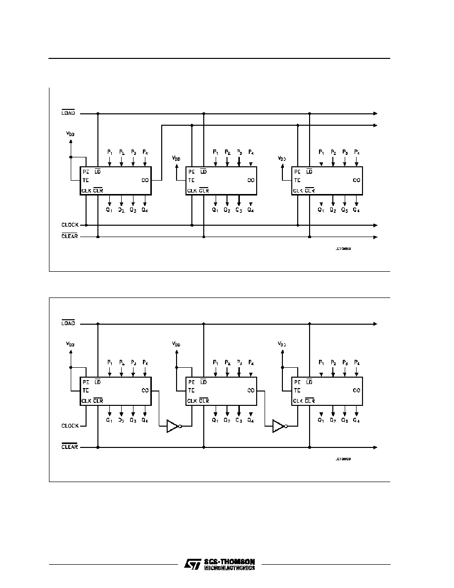
Cascading Counter Packages In The Parallel-Clocked Mode
Cascading Counter Packages In The Ripple-Clocked Mode
HCC/HCF40160B-40161B-40162B-40163B
9/15

TEST CIRCUIT
Quiescent Device Current.
Input Voltage.
Input Leakage Current.
Dinamic Power Dissipation
HCC/HCF40160B-40161B-40162-40163
10/15

Plastic DIP16 (0.25) MECHANICAL DATA
DIM.
mm
inch
MIN.
TYP.
MAX.
MIN.
TYP.
MAX.
a1
0.51
0.020
B
0.77
1.65
0.030
0.065
b
0.5
0.020
b1
0.25
0.010
D
20
0.787
E
8.5
0.335
e
2.54
0.100
e3
17.78
0.700
F
7.1
0.280
I
5.1
0.201
L
3.3
0.130
Z
1.27
0.050
P001C
HCC/HCF40160B-40161B-40162B-40163B
11/15

Ceramic DIP16/1 MECHANICAL DATA
DIM.
mm
inch
MIN.
TYP.
MAX.
MIN.
TYP.
MAX.
A
20
0.787
B
7
0.276
D
3.3
0.130
E
0.38
0.015
e3
17.78
0.700
F
2.29
2.79
0.090
0.110
G
0.4
0.55
0.016
0.022
H
1.17
1.52
0.046
0.060
L
0.22
0.31
0.009
0.012
M
0.51
1.27
0.020
0.050
N
10.3
0.406
P
7.8
8.05
0.307
0.317
Q
5.08
0.200
P053D
HCC/HCF40160B-40161B-40162-40163
12/15

SO16 (Narrow) MECHANICAL DATA
DIM.
mm
inch
MIN.
TYP.
MAX.
MIN.
TYP.
MAX.
A
1.75
0.068
a1
0.1
0.2
0.004
0.007
a2
1.65
0.064
b
0.35
0.46
0.013
0.018
b1
0.19
0.25
0.007
0.010
C
0.5
0.019
c1
45
∞
(typ.)
D
9.8
10
0.385
0.393
E
5.8
6.2
0.228
0.244
e
1.27
0.050
e3
8.89
0.350
F
3.8
4.0
0.149
0.157
G
4.6
5.3
0.181
0.208
L
0.5
1.27
0.019
0.050
M
0.62
0.024
S
8
∞
(max.)
P013H
HCC/HCF40160B-40161B-40162B-40163B
13/15

PLCC20 MECHANICAL DATA
DIM.
mm
inch
MIN.
TYP.
MAX.
MIN.
TYP.
MAX.
A
9.78
10.03
0.385
0.395
B
8.89
9.04
0.350
0.356
D
4.2
4.57
0.165
0.180
d1
2.54
0.100
d2
0.56
0.022
E
7.37
8.38
0.290
0.330
e
1.27
0.050
e3
5.08
0.200
F
0.38
0.015
G
0.101
0.004
M
1.27
0.050
M1
1.14
0.045
P027A
HCC/HCF40160B-40161B-40162-40163
14/15

Information furnished is believed to be accurate and reliable. However, SGS-THOMSON Microelectronics assumes no responsability for the
consequences of use of such information nor for any infringement of patents or other rights of third parties which may results from its use. No
license is granted by implication or otherwise under any patent or patent rights of SGS-THOMSON Microelectronics. Specifications mentioned
in this publication are subject to change without notice. This publication supersedes and replaces all information previously supplied.
SGS-THOMSON Microelectronics products are not authorized for use as critical components in life support devices or systems without express
written approval of SGS-THOMSON Microelectonics.
©
1994 SGS-THOMSON Microelectronics - All Rights Reserved
SGS-THOMSON Microelectronics GROUP OF COMPANIES
Australia - Brazil - France - Germany - Hong Kong - Italy - Japan - Korea - Malaysia - Malta - Morocco - The Netherlands -
Singapore - Spain - Sweden - Switzerland - Taiwan - Thailand - United Kingdom - U.S.A
HCC/HCF40160B-40161B-40162B-40163B
15/15