 | –≠–ª–µ–∫—Ç—Ä–æ–Ω–Ω—ã–π –∫–æ–º–ø–æ–Ω–µ–Ω—Ç: HCF40182 | –°–∫–∞—á–∞—Ç—å:  PDF PDF  ZIP ZIP |

1/10
September 2002
s
GENERATES HIGH-SPEED CARRY
ACROSS FOUR ADDERS OR ADDER
GROUPS
s
HIGH-SPEED OPERATIONAL: t
PHL
= t
PLH
=
100 ns (typ.) AT V
DD
= 10V
s
CASCADABLE FOR FAST CARRIES OVER
N BITS
s
DESIGNED FOR USE WITH HCF40181B
ALU
s
STANDARDIZED, SYMMETRICAL OUTPUT
CHARACTERISTICS
s
QUIESCENT CURRENT SPECIFIED UP TO
20V
s
INPUT LEAKAGE CURRENT
I
I
= 100nA (MAX) AT V
DD
= 18V T
A
= 25∞C
s
100% TESTED FOR QUIESCENT CURRENT
s
MEETS ALL REQUIREMENTS OF JEDEC
JESD13B "STANDARD SPECIFICATIONS
FOR DESCRIPTION OF B SERIES CMOS
DEVICES"
DESCRIPTION
HCF40182B is a monolithic integrated circuit
fabricated in Metal Oxide Semiconductor
technology available in DIP and SOP packages.
He is a high speed look-ahead carry generator
capable of anticipating a carry across four binary
adders or adder groups. HCF40182B is
cascadable to perform full look-ahead across n-bit
adders. Carry propagate-carry, and
generate-carry functions are provided as
enumerated in the terminal designation below.
HCF40182B, when used in conjunction with the
HCF40181B arithmetic logic unit (ALU), provides
full high-speed look-ahead carry capability for up
to n-bit words. Each HCF40182B generates the
look-ahead (anticipated carry) across a group of
four ALUs. In addition, other HCF40182Bs may be
emplayed to anticipate the carry across sections
of four look-ahead blocks up to n-bits.
HCF40182B
LOOK-AHEAD CARRY GENERATOR
PIN CONNECTION
ORDER CODES
PACKAGE
TUBE
T & R
DIP
HCF40182BEY
SOP
HCF40182BM1
HCF40182M013TR
DIP
SOP

HCF40182B
2/10
IINPUT EQUIVALENT CIRCUIT
PIN DESCRIPTION
FUNCTIONAL DIAGRAM
TRUTH TABLES
FOR G OUTPUT
FOR P OUTPUT
PIN No
SYMBOL
NAME AND FUNCTION
3, 1, 14, 5
G0 to G3
Carry Generate Inputs
(Active LOW)
4, 2, 15, 6
P0 to P3
Carry Propagate Inputs
(Active LOW)
13
Cn
Active-high Carry Input
12, 11, 9
Cn+x, Cn+y,
Cn+z
Active-high Carry Outputs
10
G
Carry Propagate Output
(Active LOW)
7
P
Carry Generate Output
(Active LOW)
8
Vss
Negative Supply Voltage
16
Vdd
Positive Supply Voltage
INPUTS
OUTPUT
G3
G2
G1
G0
P3
P2
P1
G
L
X
X
X
X
X
X
L
X
L
X
X
L
X
X
L
X
X
L
X
L
L
X
L
X
X
X
L
L
L
L
L
ALL OTHER COMBINATIONS
H
INPUTS
OUTPUT
P3
P2
P1
P0
P
L
L
L
L
L
ALL OTHER COMBINATIONS
H

HCF40182B
3/10
FOR Cn+x OUTPUT
FOR Cn+y OUTPUT
FOR Cn+z OUTPUT
X : Don't Care
Cn+x = G0+P0Cn
Cn+y = G1+P1G0+P1P0Cn
Cn+z = G2+P2G1+P2P1G0+P2P1P0Cn
G = G3+G3+P3G2+P3P2G1+P3P2P1G0
P = P3P2P1P0
or
Cn+x = Y0+(X0+Cn)
Cn+y = Y1+[X1+Y0(X0+Cn)]
Cn+z = Y2+{X2+Y1[X1+Y0(X0+Cn)]}
G = Y3+(X3+Y2)(X3+X2+Y1)(X3+X2+X1+Y0)
P = X3+X2+X1+X0
INPUTS
OUTPUT
G0
P0
Cn
Cn+x
L
X
X
H
X
L
H
H
ALL OTHER COMBINATIONS
L
INPUTS
OUTPUT
G1
G0
P1
P0
Cn
Cn+y
L
X
X
X
X
H
X
L
L
X
X
H
X
X
L
L
H
H
ALL OTHER COMBINATIONS
L
INPUTS
OUTPUT
G2
G1
GO
P2
P1
P0
Cn
Cn+z
L
X
X
X
X
X
X
H
X
L
X
L
X
X
X
H
X
X
L
L
L
X
X
H
X
X
X
L
L
L
H
H
ALL OTHER COMBINATIONS
L

HCF40182B
4/10
LOGIC DIAGRAM
ABSOLUTE MAXIMUM RATINGS
Absolute Maximum Ratings are those values beyond which damage to the device may occur. Functional operation under these conditions is
not implied.
All voltage values are referred to V
SS
pin voltage.
RECOMMENDED OPERATING CONDITIONS
Symbol
Parameter
Value
Unit
V
DD
Supply Voltage
-0.5 to +22
V
V
I
DC Input Voltage
-0.5 to V
DD
+ 0.5
V
I
I
DC Input Current
±
10
mA
P
D
Power Dissipation per Package
200
mW
Power Dissipation per Output Transistor
100
mW
T
op
Operating Temperature
-55 to +125
∞C
T
stg
Storage Temperature
-65 to +150
∞C
Symbol
Parameter
Value
Unit
V
DD
Supply Voltage
3 to 20
V
V
I
Input Voltage
0 to V
DD
V
T
op
Operating Temperature
-55 to 125
∞C
HCF40182B
5/10
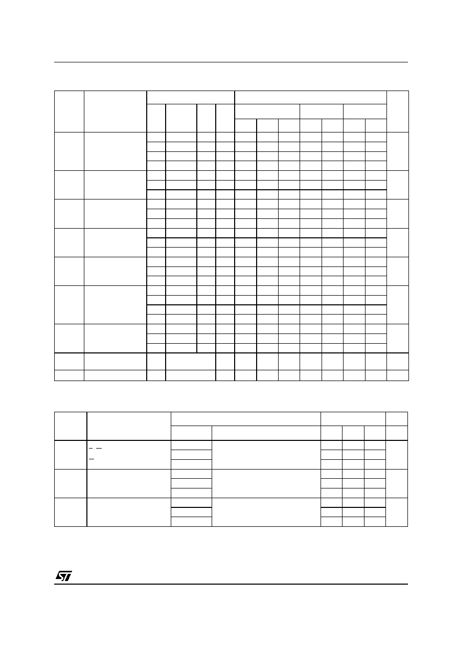
DC SPECIFICATIONS
The Noise Margin for both "1" and "0" level is: 1V min. with V
DD
=5V, 2V min. with V
DD
=10V, 2.5V min. with V
DD
=15V
DYNAMIC ELECTRICAL CHARACTERISTICS (T
amb
= 25∞C, C
L
= 50pF, R
L
= 200K
, t
r
= t
f
= 20 ns)
(*) Typical temperature coefficient for all V
DD
value is 0.3 %/∞C.
Symbol
Parameter
Test Conditions
Value
Unit
V
I
(V)
V
O
(V)
I
O
(
µ
A)
V
DD
(V)
T
A
= 25∞C
-40 to 85∞C
-55 to 125∞C
Min.
Typ.
Max.
Min.
Max.
Min.
Max.
I
L
Quiescent Current
0/5
5
0.04
5
150
150
µ
A
0/10
10
0.04
10
300
300
0/15
15
0.04
20
600
600
0/20
20
0.08
100
3000
3000
V
OH
High Level Output
Voltage
0/5
<1
5
4.95
4.95
4.95
V
0/10
<1
10
9.95
9.95
9.95
0/15
<1
15
14.95
14.95
14.95
V
OL
Low Level Output
Voltage
5/0
<1
5
0.05
0.05
0.05
V
10/0
<1
10
0.05
0.05
0.05
15/0
<1
15
0.05
0.05
0.05
V
IH
High Level Input
Voltage
0.5/4.5
<1
5
3.5
3.5
3.5
V
1/9
<1
10
7
7
7
1.5/18.5
<1
15
11
11
11
V
IL
Low Level Input
Voltage
0.5/4.5
<1
5
1.5
1.5
1.5
V
9/1
<1
10
3
3
3
1.5/18.5
<1
15
4
4
4
I
OH
Output Drive
Current
0/5
2.5
5
-1.36
-3.2
-1.1
-1.1
mA
0/5
4.6
5
-0.44
-1
-0.36
-0.36
0/10
9.5
10
-1.1
-2.6
-0.9
-0.9
0/15
13.5
15
-3.0
-6.8
-2.4
-2.4
I
OL
Output Sink
Current
0/5
0.4
5
0.44
1
0.36
0.36
mA
0/10
0.5
10
1.1
2.6
0.9
0.9
0/15
1.5
15
3.0
6.8
2.4
2.4
I
I
Input Leakage
Current
0/18
any input
18
±
10
-5
±
0.1
±
1
±
1
µ
A
C
I
Input Capacitance
any input
5
7.5
pF
Symbol
Parameter
Test Condition
Value (*)
Unit
V
DD
(V)
See Timing Chart
Min.
Typ.
Max.
t
PLH
t
PHL
Propagation Delay Time
P, G, in to P
G Out and Carry Outs
5
200
400
ns
10
100
200
15
75
150
t
PLH
t
PHL
Cn to Carry Outputs
5
240
480
ns
10
120
240
15
90
180
t
THL
t
TLH
Transition Time
5
100
200
ns
10
50
100
15
40
80