
HCC/HCF4032B
HCC/HCF4038B
June 1989
TRIPLE SERIAL ADDERS
.
INVERT INPUTS ON ALL ADDERS FOR SUM
COMPLEMENTING APPLICATIONS
.
FULLY STATIC OPERATION...DC TO 10MHz
(typ.) @ V
DD
= 10V
.
BUFFERED INPUTS AND OUTPUTS
.
SINGLE-PHASE CLOCKING
.
STANDARDIZED
SYMMETRICAL
OUTPUT
CHARACTERISTICS
.
QUIESCENT CURRENT SPECIFIED TO 20V
FOR HCC DEVICE
.
5V, 10V, AND 15V PARAMETRIC RATING
.
INPUT CURRENT OF 100nA AT 18V AND 25
∞
C
FOR HCC DEVICE
.
100% TESTED FOR QUIESCENT CURRENT
.
MEETS ALL REQUIREMENTS OF JEDEC TEN-
TATIVE STANDARD N
∞
13A, "STANDARD SPE-
CIFICATIONS FOR DESCRIPTION OF "B"
SERIES CMOS DEVICES"
DESCRIPTION
The HCC/4032B/4038B (extended temperature
range) and HCF4032B/4038B (intermediate tem-
perature range) are monolithic integrated circuits,
available in 16-lead dual in-line plastic or ceramic
package and plastic micro package.
The HCC/HCF4032B and HCC/HCF4038B types
consist of three serial adder circuits with common
CLOCK and CARRY-RESET inputs. Each adder
has two provisions for two serial DATA INPUT sig-
nals and an INVERT command signal. When the
command signal is a logical "1", the sum is com-
plemented. Data words enter the adder with the
least significant bit first ; the sign bit trails. The output
is the MOD 2 sum of the input bits plus the carry from
the previous bit position. The carry is only added at
the
positive-going
clock
transition
for
the
HCC/HCF4032B or at the negative-going clock for
the HCC/HCF4038B, thus, for spike-free operation
the input data transitions should occur as soon as
possible after the triggering edge. The CARRY is
reset to a logical "0" at the end of each word by ap-
plying a logical "1" signal to a CARRY-RESET input
one-bit-position before the application of the first bit
of the next word.
EY
(Plastic Package)
F
(Ceramic Package)
M1
(Micro Package)
C1
(Plastic Chip Carrier)
ORDER CODES :
HCC40XXBF
HCF40XXBM1
HCF40XXBEY
HCF40XXBC1
PIN CONNECTIONS
1/11
ABSOLUTE MAXIMUM RATINGS
Symbol
Parameter
Value
Unit
V
DD
*
Supply Voltage : HC C Types
H C F Types
≠ 0.5 to + 20
≠ 0.5 to + 18
V
V
V
i
Input Voltage
≠ 0.5 to V
DD
+ 0.5
V
I
I
DC Input Current (any one input)
±
10
mA
P
t o t
Total Power Dissipation (per package)
Dissipation per Output Transistor
for T
o p
= Full Package-temperature Range
200
100
mW
mW
T
o p
Operating Temperature : HCC Types
H CF Types
≠ 55 to + 125
≠ 40 to + 85
∞
C
∞
C
T
s t g
Storage Temperature
≠ 65 to + 150
∞
C
Stresses above those listed under "Absolute Maximum Ratings" may cause permanent damage to the device. This is a stress
rating only and functional operation of the device at these or any other conditions above those indicated in the operational sections
of this specification is not implied. Exposure to absolute maximum rating conditions for external periods may affect device reliability.
* All voltage values are referred to V
SS
pin voltage.
FUNCTIONAL DIAGRAM
RECOMMENDED OPERATING CONDITIONS
Symbol
Parameter
Value
Unit
V
DD
Supply Voltage : H CC Types
H C F Types
3 to 18
3 to 15
V
V
V
I
Input Voltage
0 to V
DD
V
T
o p
Operating Temperature : HCC Types
H CF Types
≠ 55 to + 125
≠ 40 to + 85
∞
C
∞
C
HCC/HCF4032B/4038B
2/11
LOGIC AND TIMING DIAGRAMS
(one of three serial adders)
WORD 1
0.0111100 =
+ 60
WORD 2
0.0110010 =
+ 50
0.1101110 = + 110
WORD 3
1.1011011 =
≠ 37
WORD 4
1.1001110 =
≠ 50
1.0101001 =
≠ 87
4032B
HCC/HCF4032B/4038B
3/11
LOGIC AND TIMING DIAGRAMS (continued)
WORD 1
1.1000011 =
≠ 61
WORD 2
1.1001101 =
≠ 51
1.0010000 = ≠ 112
WORD 3
0.0100100 =
+ 36
WORD 4
0.0110001 =
+ 49
0.1010101 =
+ 85
4038B
HCC/HCF4032B/4038B
4/11
STATIC ELECTRICAL CHARACTERISTICS (over recommended operating conditions)
Test Conditions
Value
V
I
V
O
| I
O
|
V
DD
T
Low
*
2 5
∞
C
T
High
*
Symbol
Parameter
(V)
(V)
(
µ
A)
(V)
Min.
Max. Min.
Typ.
Max. Min.
Max.
Unit
I
L
Quiescent
Current
HCC
Types
0/ 5
5
5
0.04
5
150
µ
A
0/10
10
10
0.04
10
300
0/15
15
20
0.04
20
600
0/20
20
100
0.08
100
3000
HCF
Types
0/ 5
5
20
0.04
20
150
0/10
10
40
0.04
40
300
0/15
15
80
0.04
80
600
V
OH
Output High
Voltage
0/ 5
< 1
5
4.95
4.95
4.95
V
0/10
< 1
10
9.95
9.95
9.95
0/15
< 1
15
14.95
14.95
14.95
V
OL
Output Low
Voltage
5/0
< 1
5
0.05
0.05
0.05
V
10/0
< 1
10
0.05
0.05
0.05
15/0
< 1
15
0.05
0.05
0.05
V
IH
Input High
Voltage
0.5/4.5
< 1
5
3.5
3.5
3.5
V
1/9
< 1
10
7
7
7
1.5/13.5
< 1
15
11
11
11
V
IL
Input Low
Voltage
4.5/0.5
< 1
5
1.5
1.5
1.5
V
9/1
< 1
10
3
3
3
13.5/1.5
< 1
15
4
4
4
I
OH
Output
Drive
Current
HCC
Types
0/ 5
2.5
5
≠ 2
≠ 1.6 ≠ 3.2
≠
1.15
mA
0/ 5
4.6
5
≠
0.64
≠
0.51
≠ 1
≠
0.36
0/10
9.5
10
≠ 1.6
≠ 1.3 ≠ 2.6
≠ 0.9
0/15
13.5
15
≠ 4.2
≠ 3.4 ≠ 6.8
≠ 2.4
HCF
Types
0/ 5
2.5
5
≠
1.53
≠
1.36
≠ 3.2
≠ 1.1
0/ 5
4.6
5
≠
0.52
≠
0.44
≠ 1
≠
0.36
0/10
9.5
10
≠ 1.3
≠ 1.1 ≠ 2.6
≠ 0.9
0/15
13.5
15
≠ 3.6
≠ 3.0 ≠ 6.8
≠ 2.4
I
OL
Output
Sink
Cur rent
HCC
Types
0/ 5
0.4
5
0.64
0.51
1
0.36
mA
0/10
0.5
10
1.6
1.3
2.6
0.9
0/15
1.5
15
4.2
3.4
6.8
2.4
HCF
Types
0/ 5
0.4
5
0.52
0.44
1
0.36
0/10
0.5
10
1.3
1.1
2.6
0.9
0/15
1.5
15
3.6
3.0
6.8
2.4
I
IH
, I
IL
Input
Leakage
Current
HCC
Types
0/18
Any Input
18
±
0.1
±
10
≠5
±
0.1
±
1
µ
A
HCF
Types
0/15
15
±
0.3
±
10
≠5
±
0.3
±
1
C
I
Input Capacitance
Any Input
5
7.5
pF
* T
Lo w
= ≠ 55
∞
C for HCC device : ≠ 40
∞
C for HCF device.
* T
High
= + 125
∞
C for HCC device : + 85
∞
C for HCF device.
The Noise Margin for both "1" and " 0" level is : 1V min. with V
DD
= 5V, 2V min. with V
DD
= 10V, 2.5V min. with V
DD
= 15V.
HCC/HCF4032B/4038B
5/11
DYNAMIC ELECTRICAL CHARACTERISTICS (T
amb
= 25
∞
C, C
L
= 50pF, R
L
= 200k
,
all input rise and fall time = 20ns)
Val ue
Symbol
Parameter
Test Conditions
V
D D
(V)
Min.
Typ.
Max.
Unit
t
PHL
,
t
P L H
Propagation Delay Time A, B, or
Inverter Inputs to Sum Outputs
5
260
520
ns
10
120
240
15
90
180
t
PHL
,
t
P L H
Propagation Delay Time
(clock input to sum outputs)
5
325
650
10
175
350
15
150
300
t
T HL
,
t
T HL
Transition Time
5
100
200
ns
10
50
100
15
40
80
t
h o ld
Data Input Hold Time
(clock edge to A, B, or reset
inputs)
5
120
200
ns
10
50
80
15
40
60
f
max
Maximum Clock Input Frequency
5
2.5
4.5
MHz
10
5
10
15
7.5
15
t
r
, t
f
*
Clock Input Rise or Fall Time
5
500
µ
s
10
500
15
500
* If more than one unit is cascaded t
r
should be made less than or equal to the sum of the transition time and the fixed propa-
gation delay of the output of the driving state for the estimated capacitive load.
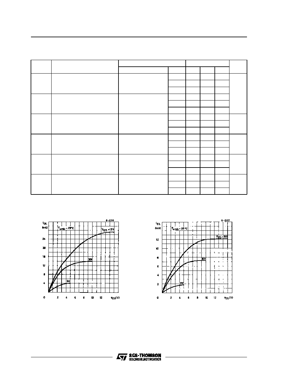
Typical Output Low (sink) Current.
Minimum Output Low (sink) Current Charac-
teristics.
HCC/HCF4032B/4038B
6/11

Typical Output High (source) Current Charac-
teristics.
Minimum Output High (source) Current Charac-
teristics.
TEST CIRCUITS
Quiescent Device Current.
Input Voltage.
Input Current.
HCC/HCF4032B/4038B
7/11
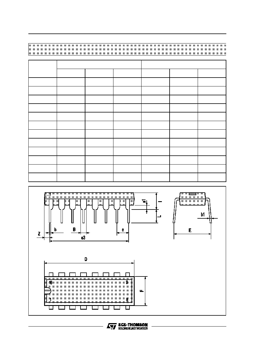
Plastic DIP16 (0.25) MECHANICAL DATA
DIM.
mm
inch
MIN.
TYP.
MAX.
MIN.
TYP.
MAX.
a1
0.51
0.020
B
0.77
1.65
0.030
0.065
b
0.5
0.020
b1
0.25
0.010
D
20
0.787
E
8.5
0.335
e
2.54
0.100
e3
17.78
0.700
F
7.1
0.280
I
5.1
0.201
L
3.3
0.130
Z
1.27
0.050
P001C
HCC/HCF4032B/4038B
8/11

Ceramic DIP16/1 MECHANICAL DATA
DIM.
mm
inch
MIN.
TYP.
MAX.
MIN.
TYP.
MAX.
A
20
0.787
B
7
0.276
D
3.3
0.130
E
0.38
0.015
e3
17.78
0.700
F
2.29
2.79
0.090
0.110
G
0.4
0.55
0.016
0.022
H
1.17
1.52
0.046
0.060
L
0.22
0.31
0.009
0.012
M
0.51
1.27
0.020
0.050
N
10.3
0.406
P
7.8
8.05
0.307
0.317
Q
5.08
0.200
P053D
HCC/HCF4032B/4038B
9/11

PLCC20 MECHANICAL DATA
DIM.
mm
inch
MIN.
TYP.
MAX.
MIN.
TYP.
MAX.
A
9.78
10.03
0.385
0.395
B
8.89
9.04
0.350
0.356
D
4.2
4.57
0.165
0.180
d1
2.54
0.100
d2
0.56
0.022
E
7.37
8.38
0.290
0.330
e
1.27
0.050
e3
5.08
0.200
F
0.38
0.015
G
0.101
0.004
M
1.27
0.050
M1
1.14
0.045
P027A
HCC/HCF4032B/4038B
10/11
Information furnished is believed to be accurate and reliable. However, SGS-THOMSON Microelectronics assumes no responsability for the
consequences of use of such information nor for any infringement of patents or other rights of third parties which may results from its use. No
license is granted by implication or otherwise under any patent or patent rights of SGS-THOMSON Microelectronics. Specifications mentioned
in this publication are subject to change without notice. This publication supersedes and replaces all information previously supplied.
SGS-THOMSON Microelectronics products are not authorized for use as critical components in life support devices or systems without express
written approval of SGS-THOMSON Microelectonics.
©
1994 SGS-THOMSON Microelectronics - All Rights Reserved
SGS-THOMSON Microelectronics GROUP OF COMPANIES
Australia - Brazil - France - Germany - Hong Kong - Italy - Japan - Korea - Malaysia - Malta - Morocco - The Netherlands -
Singapore - Spain - Sweden - Switzerland - Taiwan - Thailand - United Kingdom - U.S.A
HCC/HCF4032B/4038B
11/11