1/11
September 2003
s
QUIESCENT CURRENT SPECIFIED UP TO
20V
s
3-LEVEL OUTPUTS WITH COMMON
OUTPUT ENABLE
s
SEPARATE SET AND RESET INPUT FOR
EACH LATCH
s
5V, 10V AND 15V PARAMETRIC RATINGS
s
INPUT LEAKAGE CURRENT
I
I
= 100nA (MAX) AT V
DD
= 18V T
A
= 25∞C
s
100% TESTED FOR QUIESCENT CURRENT
s
MEETS ALL REQUIREMENTS OF JEDEC
JESD13B "STANDARD SPECIFICATIONS
FOR DESCRIPTION OF B SERIES CMOS
DEVICES"
DESCRIPTION
The HCF4043B is a monolithic integrated circuit
fabricated
in
Metal
Oxide
Semiconductor
technology available in DIP and SOP packages.
The HCF4043B is a quad cross-coupled 3-state
CMOS NOR latch.
Each latch has a separate Q output and individual
SET and RESET input. The Q outputs are
controlled by a common ENABLE input. A logic "1"
or "high" on the ENABLE inputs connects the latch
states to the Q outputs. A logic "0" or "low" on the
ENABLE input disconnects the latch states from
the Q outputs, resulting in an open circuit
condition on the Q outputs. The open circuit
feature allows common bussing of the outputs.
HCF4043B
QUAD NOR 3-STATE R-S LATCH
PIN CONNECTION
ORDER CODES
PACKAGE
TUBE
T & R
DIP
HCF4043BEY
SOP
HCF4043BM1
HCF4043M013TR
DIP
SOP

HCF4043B
3/11
LOGIC DIAGRAM
ABSOLUTE MAXIMUM RATINGS
Absolute Maximum Ratings are those values beyond which damage to the device may occur. Functional operation under these conditions is
not implied.
All voltage values are referred to V
SS
pin voltage.
RECOMMENDED OPERATING CONDITIONS
Symbol
Parameter
Value
Unit
V
DD
Supply Voltage
-0.5 to +22
V
V
I
DC Input Voltage
-0.5 to V
DD
+ 0.5
V
I
I
DC Input Current
±
10
mA
P
D
Power Dissipation per Package
200
mW
Power Dissipation per Output Transistor
100
mW
T
op
Operating Temperature
-55 to +125
∞C
T
stg
Storage Temperature
-65 to +150
∞C
Symbol
Parameter
Value
Unit
V
DD
Supply Voltage
3 to 20
V
V
I
Input Voltage
0 to V
DD
V
T
op
Operating Temperature
-55 to 125
∞C

HCF4043B
5/11
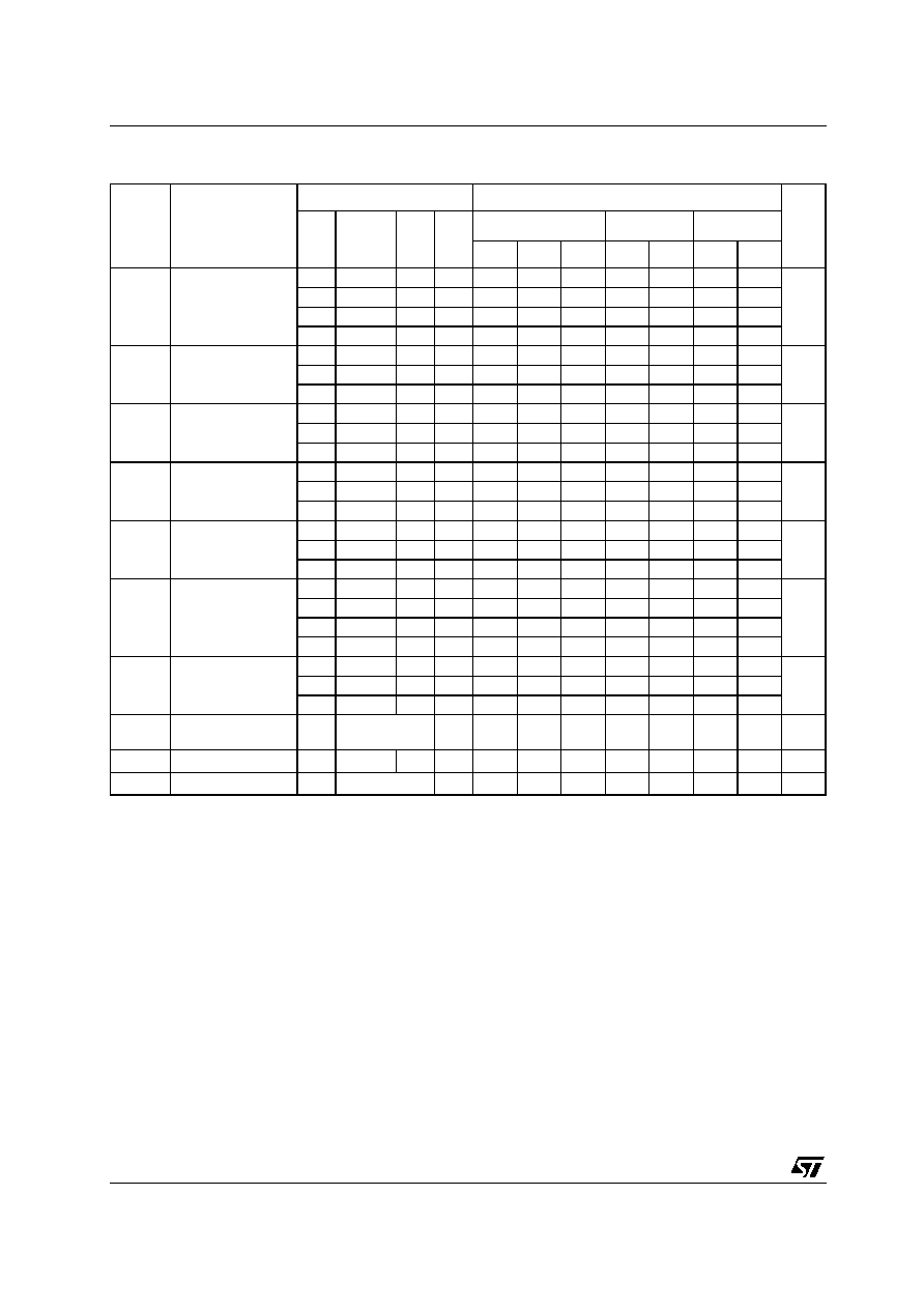
DYNAMIC ELECTRICAL CHARACTERISTICS (T
amb
= 25∞C, C
L
= 50pF, R
L
= 200K
, t
r
= t
f
= 20 ns)
(*) Typical temperature coefficient for all V
DD
value is 0.3%/∞C.
TYPICAL APPLICATIONS
MULTIPLE BUS STORAGE
Symbol
Parameter
Test Condition
Value (*)
Unit
V
DD
(V)
Min.
Typ.
Max.
t
PLH
t
PHL
Propagation Delay Time
(SET or RESET to Q)
5
150
300
ns
10
70
140
15
50
100
t
PZH
t
PZL
3-State Propagation Delay
Time (Enable to Q)
5
115
230
ns
10
55
110
15
40
80
t
PLZ
t
PHZ
3-State Propagation Delay
Time (Disable to Q)
5
90
180
ns
10
50
100
15
35
70
t
TLH
t
THL
Transition Time
5
100
200
ns
10
50
100
15
40
80
t
W
Pulse Width (Set or Reset)
5
160
80
ns
10
80
40
15
40
20