1/10
September 2003
s
QUIESCENT CURRENT SPECIFIED UP TO
20V
s
3-LEVEL OUTPUTS WITH COMMON
OUTPUT ENABLE
s
SEPARATE SET AND RESET INPUT FOR
EACH LATCH
s
5V, 10V AND 15V PARAMETRIC RATINGS
s
INPUT LEAKAGE CURRENT
I
I
= 100nA (MAX) AT V
DD
= 18V T
A
= 25∞C
s
100% TESTED FOR QUIESCENT CURRENT
s
MEETS ALL REQUIREMENTS OF JEDEC
JESD13B "STANDARD SPECIFICATIONS
FOR DESCRIPTION OF B SERIES CMOS
DEVICES"
DESCRIPTION
The HCF4044B is a monolithic integrated circuit
fabricated
in
Metal
Oxide
Semiconductor
technology available in DIP and SOP packages.
The HCF4044B is a quad cross-coupled 3-state
CMOS NAND latch.
Each latch has a separate Q output and individual
SET and RESET input. The Q outputs are
controlled by a common ENABLE input. A logic "1"
or "high" on the ENABLE inputs connects the latch
states to the Q outputs. A logic "0" or "low" on the
ENABLE input disconnects the latch states from
the Q outputs, resulting in an open circuit
condition on the Q outputs. The open circuit
feature allows common bussing of the outputs.
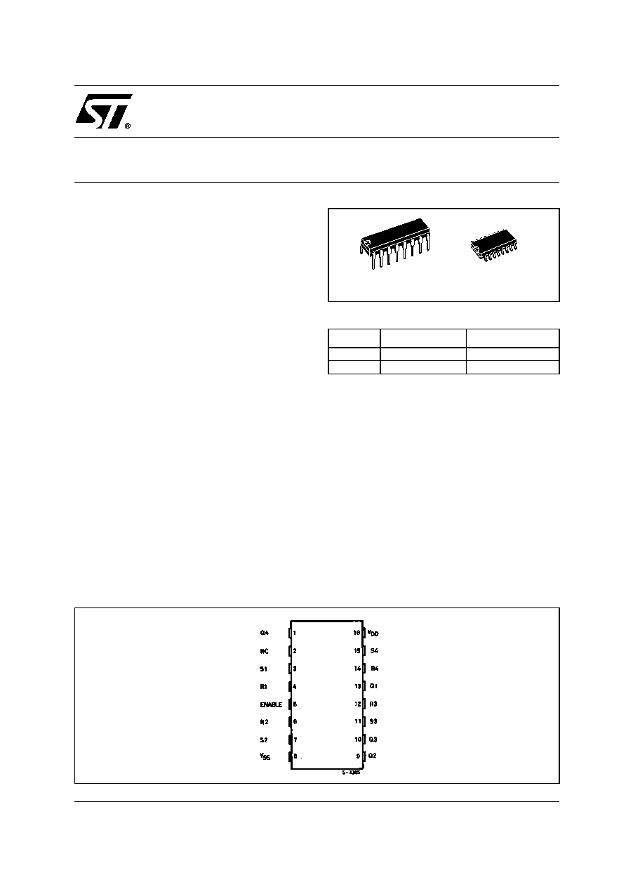
HCF4044B
QUAD NAND 3-STATE R-S LATCH
PIN CONNECTION
ORDER CODES
PACKAGE
TUBE
T & R
DIP
HCF4044BEY
SOP
HCF4044BM1
HCF4044M013TR
DIP
SOP
HCF4044B
2/10
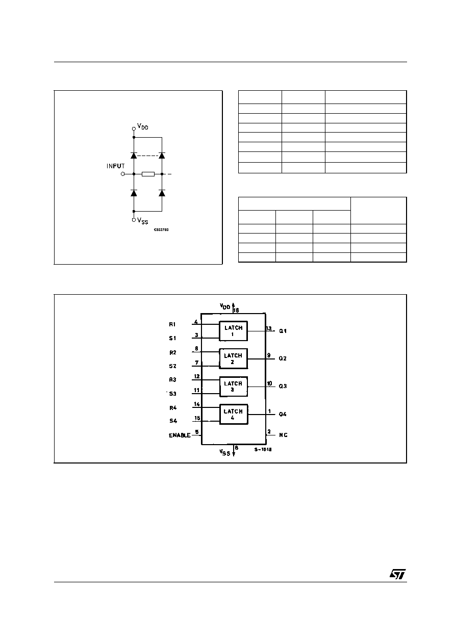
INPUT EQUIVALENT CIRCUIT
PIN DESCRIPTION
TRUTH TABLE
X : Don't Care; Z = High Impedance; Latched: No change
FUNCTIONAL DIAGRAM
PIN No
SYMBOL
NAME AND FUNCTION
4, 6, 12, 14
S1 to S4
Set Inputs
3, 7, 11, 15
R1 to R4
Reset Inputs
5
ENABLE
Enable Input
13, 9, 10, 1
Q1 to Q4
Outputs
2
NC
Not Connected
8
V
SS
Negative Supply Voltage
16
V
DD
Positive Supply Voltage
INPUTS
OUTPUT Qn
ENABLE
Sn
Rn
L
X
X
Z
H
L
H
H
H
X
L
L
H
H
H
LATCHED
HCF4044B
3/10
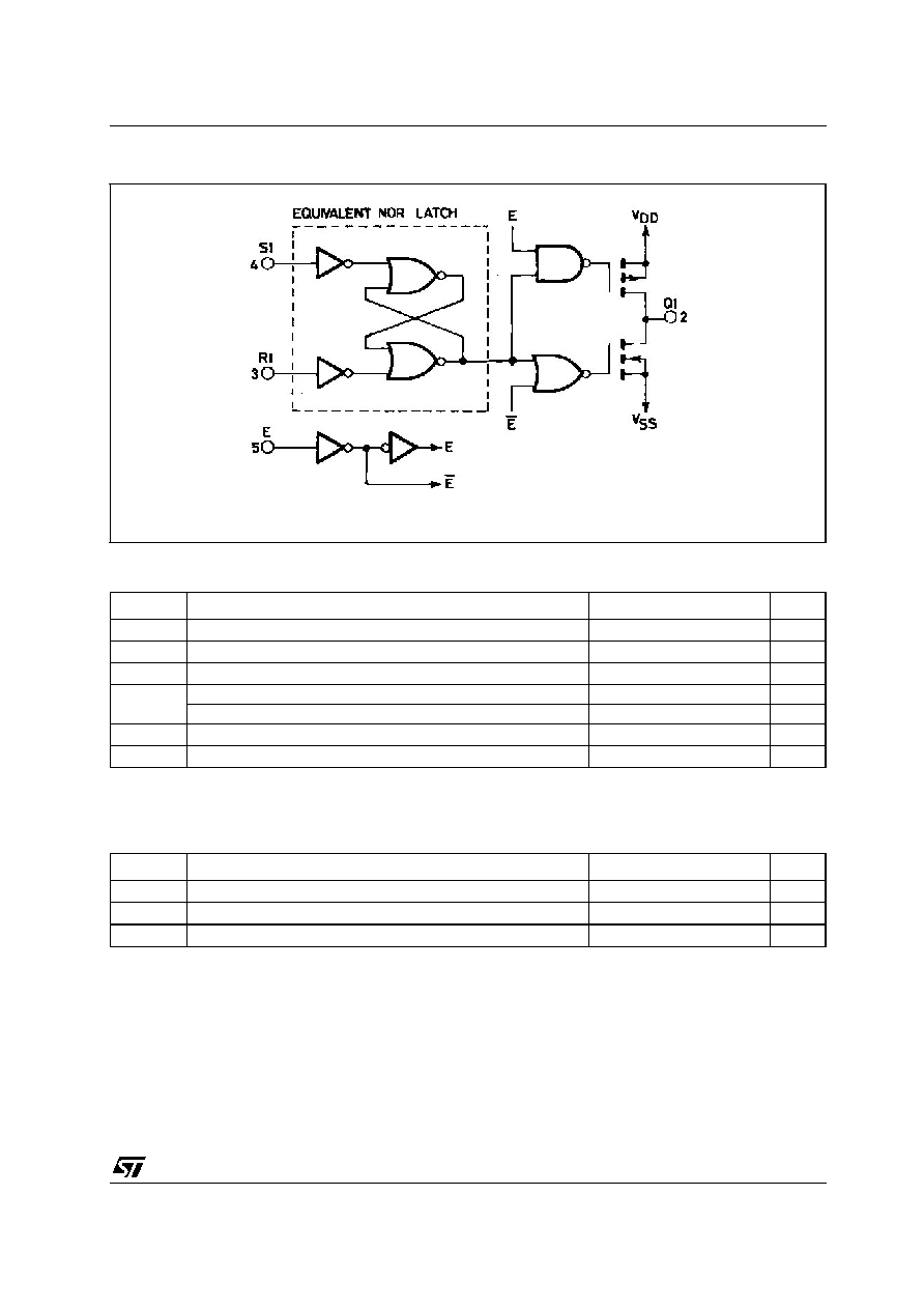
LOGIC DIAGRAM
ABSOLUTE MAXIMUM RATINGS
Absolute Maximum Ratings are those values beyond which damage to the device may occur. Functional operation under these conditions is
not implied.
All voltage values are referred to V
SS
pin voltage.
RECOMMENDED OPERATING CONDITIONS
Symbol
Parameter
Value
Unit
V
DD
Supply Voltage
-0.5 to +22
V
V
I
DC Input Voltage
-0.5 to V
DD
+ 0.5
V
I
I
DC Input Current
±
10
mA
P
D
Power Dissipation per Package
200
mW
Power Dissipation per Output Transistor
100
mW
T
op
Operating Temperature
-55 to +125
∞C
T
stg
Storage Temperature
-65 to +150
∞C
Symbol
Parameter
Value
Unit
V
DD
Supply Voltage
3 to 20
V
V
I
Input Voltage
0 to V
DD
V
T
op
Operating Temperature
-55 to 125
∞C
HCF4044B
4/10
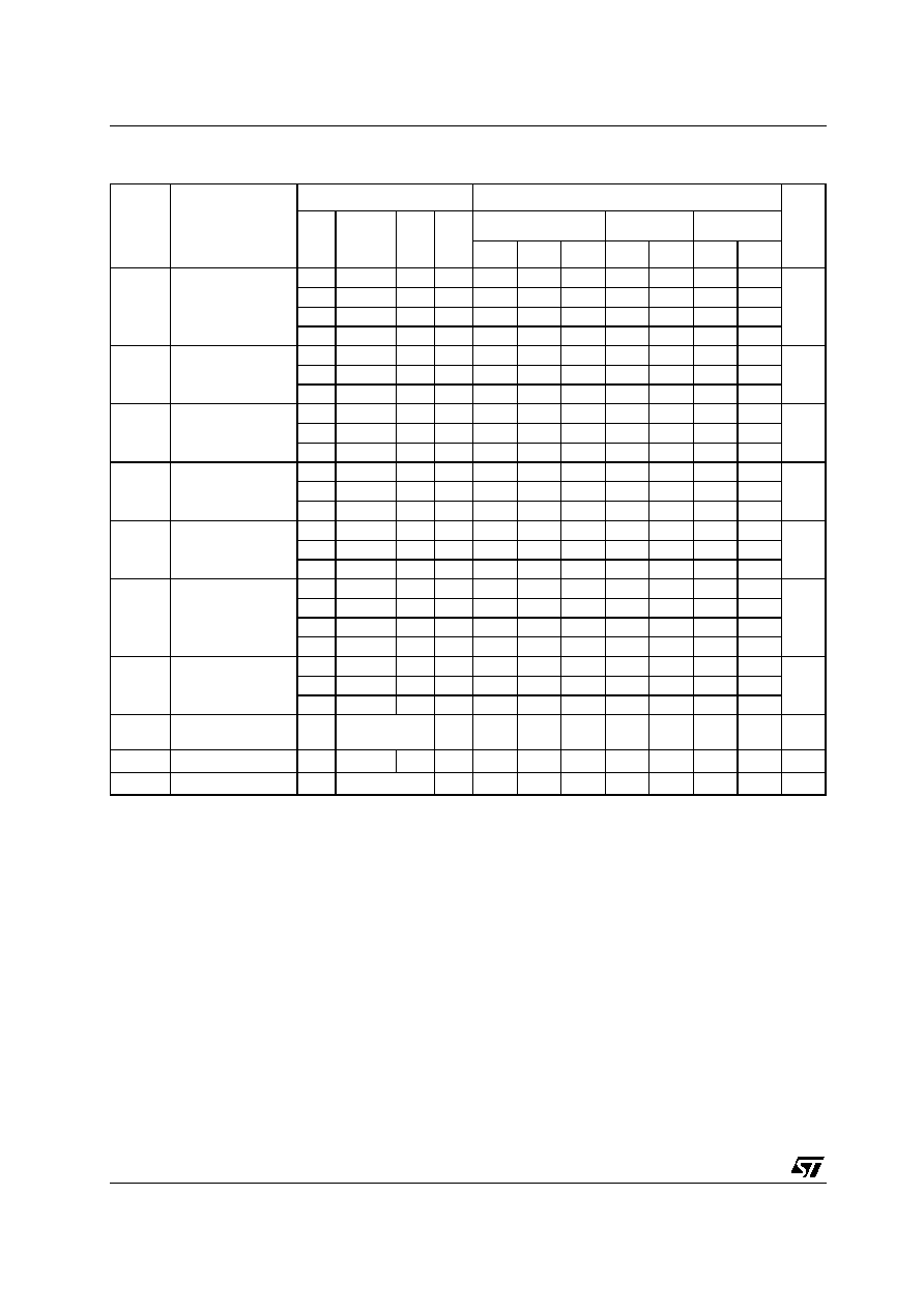
DC SPECIFICATIONS
The Noise Margin for both "1" and "0" level is: 1V min. with V
DD
=5V, 2V min. with V
DD
=10V, 2.5V min. with V
DD
=15V
Symbol
Parameter
Test Condition
Value
Unit
V
I
(V)
V
O
(V)
|I
O
|
(
µ
A)
V
DD
(V)
T
A
= 25∞C
-40 to 85∞C
-55 to 125∞C
Min.
Typ.
Max.
Min.
Max.
Min.
Max.
I
L
Quiescent Current
0/5
5
0.02
1
30
30
µ
A
0/10
10
0.02
2
60
60
0/15
15
0.02
4
120
120
0/20
20
0.04
20
600
600
V
OH
High Level Output
Voltage
0/5
<1
5
4.95
4.95
4.95
V
0/10
<1
10
9.95
9.95
9.95
0/15
<1
15
14.95
14.95
14.95
V
OL
Low Level Output
Voltage
5/0
<1
5
0.05
0.05
0.05
V
10/0
<1
10
0.05
0.05
0.05
15/0
<1
15
0.05
0.05
0.05
V
IH
High Level Input
Voltage
0.5/4.5
<1
5
3.5
3.5
3.5
V
1/9
<1
10
7
7
7
1.5/13.5
<1
15
11
11
11
V
IL
Low Level Input
Voltage
4.5/0.5
<1
5
1.5
1.5
1.5
V
9/1
<1
10
3
3
3
13.5/1.5
<1
15
4
4
4
I
OH
Output Drive
Current
0/5
2.5
<1
5
-1.36
-3.2
-1.15
-1.1
mA
0/5
4.6
<1
5
-0.44
-1
-0.36
-0.36
0/10
9.5
<1
10
-1.1
-2.6
-0.9
-0.9
0/15
13.5
<1
15
-3.0
-6.8
-2.4
-2.4
I
OL
Output Sink
Current
0/5
0.4
<1
5
0.44
1
0.36
0.36
mA
0/10
0.5
<1
10
1.1
2.6
0.9
0.9
0/15
1.5
<1
15
3.0
6.8
2.4
2.4
I
I
Input Leakage
Current
0/18
Any Input
18
±
10
-5
±
0.1
±
1
±
1
µ
A
I
OZ
3-State Output
0/18
0/18
18
±
10
-4
±
0.4
±
12
±
12
µ
A
C
I
Input Capacitance
Any Input
5
7.5
pF

HCF4044B
5/10
DYNAMIC ELECTRICAL CHARACTERISTICS (T
amb
= 25∞C, C
L
= 50pF, R
L
= 200K
, t
r
= t
f
= 20 ns)
(*) Typical temperature coefficient for all V
DD
value is 0.3%/∞C.
TEST CIRCUIT
C
L
= 50pF or equivalent (includes jig and probe capacitance)
R
L
= 200K
R
T
= Z
OUT
of pulse generator (typically 50
)
Symbol
Parameter
Test Condition
Value (*)
Unit
V
DD
(V)
Min.
Typ.
Max.
t
PLH
t
PHL
Propagation Delay Time
(SET or RESET to Q)
5
150
300
ns
10
70
140
15
50
100
t
PZH
t
PZL
3-State Propagation Delay
Time (Enable to Q)
5
115
230
ns
10
55
110
15
40
80
t
PLZ
t
PHZ
3-State Propagation Delay
Time (Disable to Q)
5
90
180
ns
10
50
100
15
35
70
t
TLH
t
THL
Transition Time
5
100
200
ns
10
50
100
15
40
80
t
W
Pulse Width (Set or Reset)
5
160
80
ns
10
80
40
15
40
20

HCF4044B
6/10
WAVEFORM 1: PROPAGATION DELAY TIMES (f=1MHz; 50% duty cycle)
WAVEFORM 2: OUTPUT ENABLE AND DISABLE TIMES (f=1MHz; 50% duty cycle)
HCF4044B
7/10
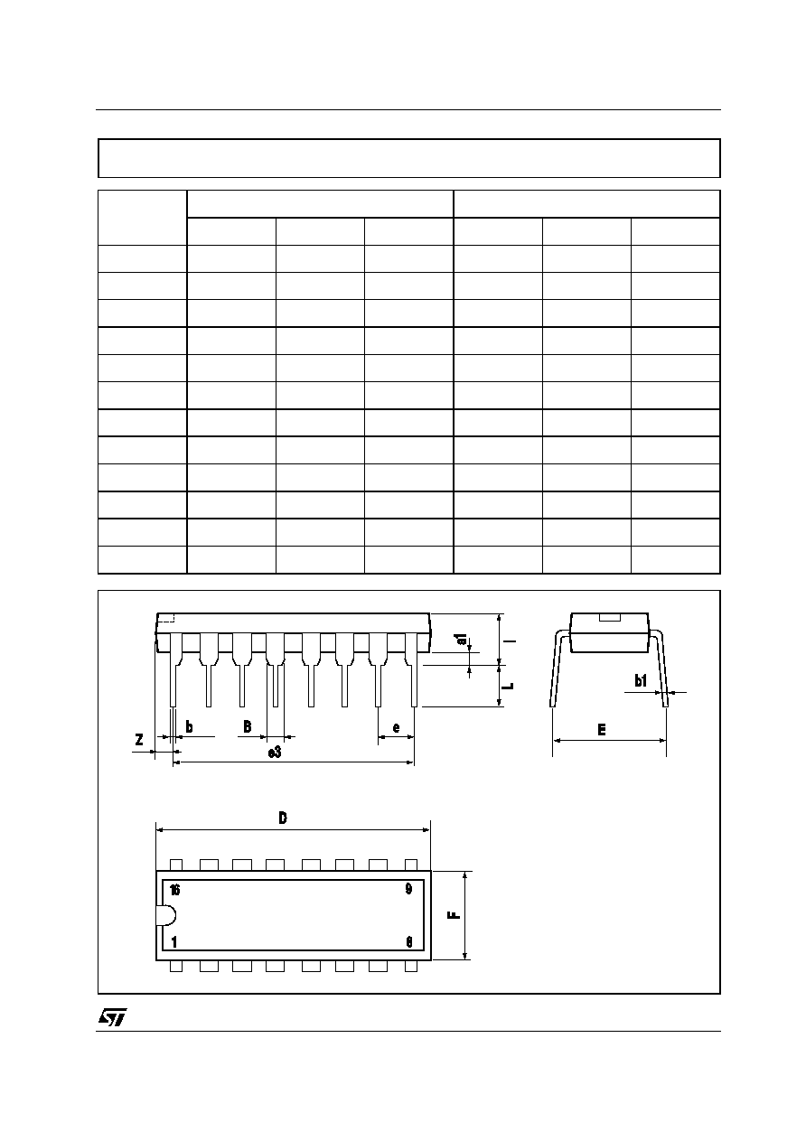
DIM.
mm.
inch
MIN.
TYP
MAX.
MIN.
TYP.
MAX.
a1
0.51
0.020
B
0.77
1.65
0.030
0.065
b
0.5
0.020
b1
0.25
0.010
D
20
0.787
E
8.5
0.335
e
2.54
0.100
e3
17.78
0.700
F
7.1
0.280
I
5.1
0.201
L
3.3
0.130
Z
1.27
0.050
Plastic DIP-16 (0.25) MECHANICAL DATA
P001C

HCF4044B
8/10
DIM.
mm.
inch
MIN.
TYP
MAX.
MIN.
TYP.
MAX.
A
1.75
0.068
a1
0.1
0.2
0.004
0.008
a2
1.65
0.064
b
0.35
0.46
0.013
0.018
b1
0.19
0.25
0.007
0.010
C
0.5
0.019
c1
45∞ (typ.)
D
9.8
10
0.385
0.393
E
5.8
6.2
0.228
0.244
e
1.27
0.050
e3
8.89
0.350
F
3.8
4.0
0.149
0.157
G
4.6
5.3
0.181
0.208
L
0.5
1.27
0.019
0.050
M
0.62
0.024
S
8
∞ (max.)
SO-16 MECHANICAL DATA
PO13H

HCF4044B
9/10
DIM.
mm.
inch
MIN.
TYP
MAX.
MIN.
TYP.
MAX.
A
330
12.992
C
12.8
13.2
0.504
0.519
D
20.2
0.795
N
60
2.362
T
22.4
0.882
Ao
6.45
6.65
0.254
0.262
Bo
10.3
10.5
0.406
0.414
Ko
2.1
2.3
0.082
0.090
Po
3.9
4.1
0.153
0.161
P
7.9
8.1
0.311
0.319
Tape & Reel SO-16 MECHANICAL DATA

HCF4044B
10/10
Information furnished is believed to be accurate and reliable. However, STMicroelectronics assumes no responsibility for the
consequences of use of such information nor for any infringement of patents or other rights of third parties which may result from
its use. No license is granted by implication or otherwise under any patent or patent rights of STMicroelectronics. Specifications
mentioned in this publication are subject to change without notice. This publication supersedes and replaces all information
previously supplied. STMicroelectronics products are not authorized for use as critical components in life support devices or
systems without express written approval of STMicroelectronics.
The ST logo is a registered trademark of STMicroelectronics
All other names are the property of their respective owners
© 2003 STMicroelectronics - All Rights Reserved
STMicroelectronics GROUP OF COMPANIES
Australia - Belgium - Brazil - Canada - China - Czech Republic - Finland - France - Germany - Hong Kong - India - Israel - Italy - Japan -
Malaysia - Malta - Morocco - Singapore - Spain - Sweden - Switzerland - United Kingdom - United States.
http://www.st.com