 | –≠–ª–µ–∫—Ç—Ä–æ–Ω–Ω—ã–π –∫–æ–º–ø–æ–Ω–µ–Ω—Ç: HCF4069UB | –°–∫–∞—á–∞—Ç—å:  PDF PDF  ZIP ZIP |
HCC/HCF4069UB
June 1989
HEX INVERTER
DESCRIPTION
.
MEDIUM-SPEED OPERATION
≠ t
PHL
, t
PLH
= 30ns (typ.) AT 10V
.
QUIESCENT CURRENT SPECIFIED TO 20V
FOR HCC DEVICE
.
STANDARDIZED
SYMMETRICAL
OUTPUT
CHARACTERISTICS
.
5V, 10V, AND 15V PARAMETRIC RATINGS
.
INPUT CURRENT OF 100nA AT 18V AND
25
∞
C FOR HCC DEVICE
.
100% TESTED FOR QUIESCENT CURRENT
.
MEETS ALL REQUIREMENTS OF JEDEC TEN-
TATIVE STANDARD N
∞
13A, "STANDARD SPE-
CIFICATIONS FOR DESCRIPTION OF "B"
SERIES CMOS DEVICES"
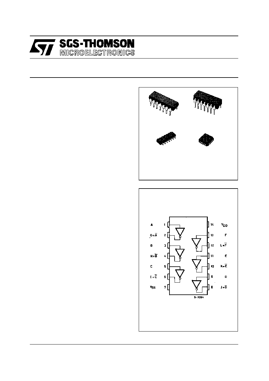
The HCC4069UB (extended temperature range)
and HCF4069UB (intermediate temperature range)
are monolithic integrated circuit, available in 14-lead
dual in-line plastic or ceramic package and plastic
micro package.
The HCC/HCF4069UB consists of six COS/MOS in-
verter circuits. This device is intended for all general-
purpose
inverter
applications
where
the
medium-power TTL-drive and logic-level-conver-
sion capabilities of circuits such as HCC/HCF4049B
Hex Inverter/Buffers are not required.
EY
(Plastic Package)
F
(Ceramic Frit Seal Package)
M1
(Micro Package)
C1
(Plastic Chip Carrier)
ORDER CODES :
HCC4069UBF
HCF4069UBM1
HCF4069UBEY
HCF4069UBC1
PIN CONNECTIONS
1/12
ABSOLUTE MAXIMUM RATINGS
Symbol
Parameter
Value
Unit
V
DD
*
Supply Voltage : HCC Types
HC F Types
≠ 0.5 to + 20
≠ 0.5 to + 18
V
V
V
i
Input Voltage
≠ 0.5 to V
DD
+ 0.5
V
I
I
DC Input Current (any one input)
±
10
mA
P
t o t
Total Power Dissipation (per package)
Dissipation per Output Transistor
for Top = Full Package-temperature Range
200
100
mW
mW
T
o p
Operating Temperature : HCC Types
H CF Types
≠ 55 to + 125
≠ 40 to + 85
∞
C
∞
C
T
s t g
Storage Temperature
≠ 65 to + 150
∞
C
Stresses above those listed under "Absolute Maximum Ratings" may cause permanent damage to the device. This is a stress
rating only and functional operation of the device at these or any other conditions above those indicated in the operational sec-
tions of this specifi cation is not implied. Exposure to absolute maximum rating conditions for external periods may affect device
reliability.
* All voltage values are referred to V
SS
pin voltage.
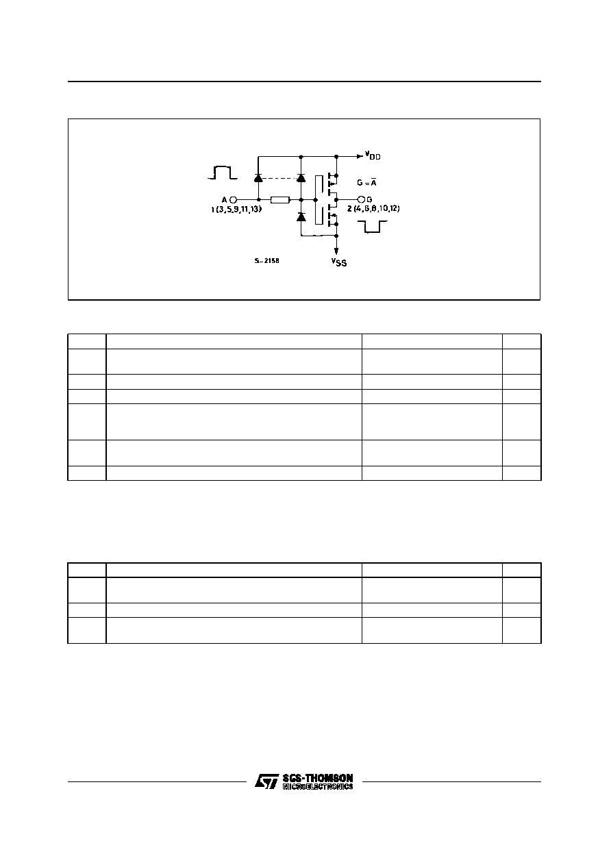
SCHEMATIC DIAGRAM OF ONE OF SIX IDENTICAL INVERTERS.
RECOMMENDED OPERATING CONDITIONS
Symbol
Parameter
Value
Unit
V
DD
Supply Voltage : HCC Types
HC F Types
3 to 18
3 to 15
V
V
V
I
Input Voltage
0 to V
DD
V
T
o p
Operating Temperature : HCC Types
H CF Types
≠ 55 to + 125
≠ 40 to + 85
∞
C
∞
C
HCC/HCF4069UB
2/12
STATIC ELECTRICAL CHARACTERISTICS (over recommended operating conditions)
Test Conditions
Value
V
I
V
O
|I
O
|
V
D D
T
L o w
*
25
∞
C
T
Hi g h
*
Symbol
Parameter
(V)
(V)
(
µ
A)
(V)
Min. Max. Min. Typ. Max. Min. Max.
Unit
I
L
Quiescent
Current
HCC
Types
0/ 5
5
0.25
0.01
0.25
7.5
µ
A
0/10
10
0.5
0.01
0.5
15
0/15
15
1
0.01
1
30
0/20
20
5
0.02
5
150
HCF
Types
0/ 5
5
1
0.01
1
7.5
0/10
10
2
0.01
2
15
0/15
15
4
0.01
4
30
V
O H
Output High
Voltage
0/ 5
< 1
5
4.95
4.95
4.95
V
0/10
< 1
10
9.95
9.95
9.95
0/15
< 1
15
14.95
14.95
14.95
V
O L
Output Low
Voltage
5/0
< 1
5
0.05
0.05
0.05
V
10/0
< 1
10
0.05
0.05
0.05
15/0
< 1
15
0.05
0.05
0.05
V
IH
Input High
Voltage
0.5/4.5
< 1
5
4
4
4
V
1/9
< 1
10
8
8
8
1.5/13.5
< 1
15
12.5
12.5
12.5
V
IL
Input Low
Voltage
4.5/0.5
< 1
5
1
1
1
V
9/1
< 1
10
2
2
2
13.5/1.5
< 1
15
2.5
2.5
2.5
I
O H
Output
Drive
Current
HCC
Types
0/ 5
2.5
5
≠ 2
≠ 1.6 ≠ 3.2
≠ 1.15
mA
0/ 5
4.6
5
≠ 0.64
≠ 0.51 ≠ 1
≠ 0.36
0/10
9.5
10
≠ 1.6
≠ 1.3 ≠ 2.6
≠ 0.9
0/15
13.5
15
≠ 4.2
≠ 3.4 ≠ 6.8
≠ 2.4
HCF
Types
0/ 5
2.5
5
≠ 1.53
≠ 1.36 ≠ 3.2
≠ 1.1
0/ 5
4.6
5
≠ 0.52
≠ 0.44 ≠ 1
≠ 0.36
0/10
9.5
10
≠ 1.3
≠ 1.1 ≠ 2.6
≠ 0.9
0/15
13.5
15
≠ 3.6
≠ 3.0 ≠ 6.8
≠ 2.4
I
O L
Output
Sink
Current
HCC
Types
0/ 5
0.4
5
0.64
0.51
1
0.36
mA
0/10
0.5
10
1.6
1.3
2.6
0.9
0/15
1.5
15
4.2
3.4
6.8
2.4
HCF
Types
0/ 5
0.4
5
0.52
0.44
1
0.36
0/10
0.5
10
1.3
1.1
2.6
0.9
0/15
1.5
15
3.6
3.0
6.8
2.4
I
IH
, I
IL
Input
Leakage
Current
HCC
Types
0/18
Any Input
18
±
0.1
±
10
≠ 5
±
0.1
±
1
µ
A
HCF
Types
0/15
15
±
0.3
±
10
≠ 5
±
0.3
±
1
C
I
Input Capacitance
Any Input
5
7.5
pF
* T
Lo w
= ≠ 55
∞
C for HCC device : ≠ 40
∞
C for HCF device.
* T
High
= + 125
∞
C for HCC device : + 85
∞
C for HCF device.
The Noise Margin for both " 1" and " 0" level is : 1V min. with V
DD
= 5V, 2V min. with V
DD
= 10V, 2.5V min. with V
DD
= 15V.
HCC/HCF4069UB
3/12
DYNAMIC ELECTRICAL CHARACTERISTICS (T
amb
= 25
∞
C, C
L
= 50pF, R
L
= 200k
,
typical temperature coefficient for all V
DD
= 0.3%/
∞
C values, all input rise and fall time = 20ns)
Val ue
Symbol
Parameter
Test Conditions
V
D D
(V)
Min.
Typ.
Max.
Unit
t
P L H
, t
P HL
Propagation Delay Time
5
55
110
ns
10
30
60
15
25
50
t
TL H
, t
T HL
Transition Time
5
100
200
ns
10
50
100
15
40
80
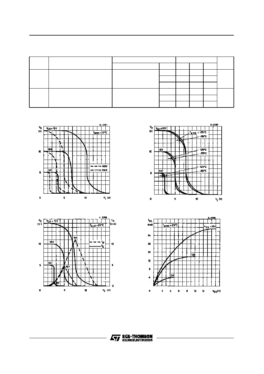
Typical Current and Voltage Transfer Charac-
teristics.
Minimum and Maximum Voltage Transfer Charac-
teristics.
Typical Voltage Transfer Characteristics as a
Function of Temperature.
Typical Output Low (sink) Current Characteristics.
HCC/HCF4069UB
4/12

Typical Output High (source) Current Charac-
teristics.
Minimum Output Low (sink) Current Charac-
teristics.
Typical Propagation Delay Time vs. Load Capacit-
ance.
Minimum Output High (source) Current Charac-
teristics.
Typical Transition Time vs. Load Capacitance.
Typical Propagation Delay Time vs. Load Capacit-
ance.
HCC/HCF4069UB
5/12