 | –≠–ª–µ–∫—Ç—Ä–æ–Ω–Ω—ã–π –∫–æ–º–ø–æ–Ω–µ–Ω—Ç: HCF4076 | –°–∫–∞—á–∞—Ç—å:  PDF PDF  ZIP ZIP |

1/9
September 2002
s
THREE STATE OUTPUTS
s
INPUT DISABLE WITHOUT GATING THE
CLOCK
s
GATED OUTPUT CONTROL LINES FOR
ENABLING OR DISABLING THE OUTPUTS
s
BUFFERED INPUTS AND OUTPUTS
s
QUIESCENT CURRENT SPECIFIED UP TO
20V
s
5V, 10V AND 15V PARAMETRIC RATINGS
s
INPUT LEAKAGE CURRENT
I
I
= 100nA (MAX) AT V
DD
= 18V T
A
= 25∞C
s
100% TESTED FOR QUIESCENT CURRENT
s
MEETS ALL REQUIREMENTS OF JEDEC
JESD13B "STANDARD SPECIFICATIONS
FOR DESCRIPTION OF B SERIES CMOS
DEVICES"
DESCRIPTION
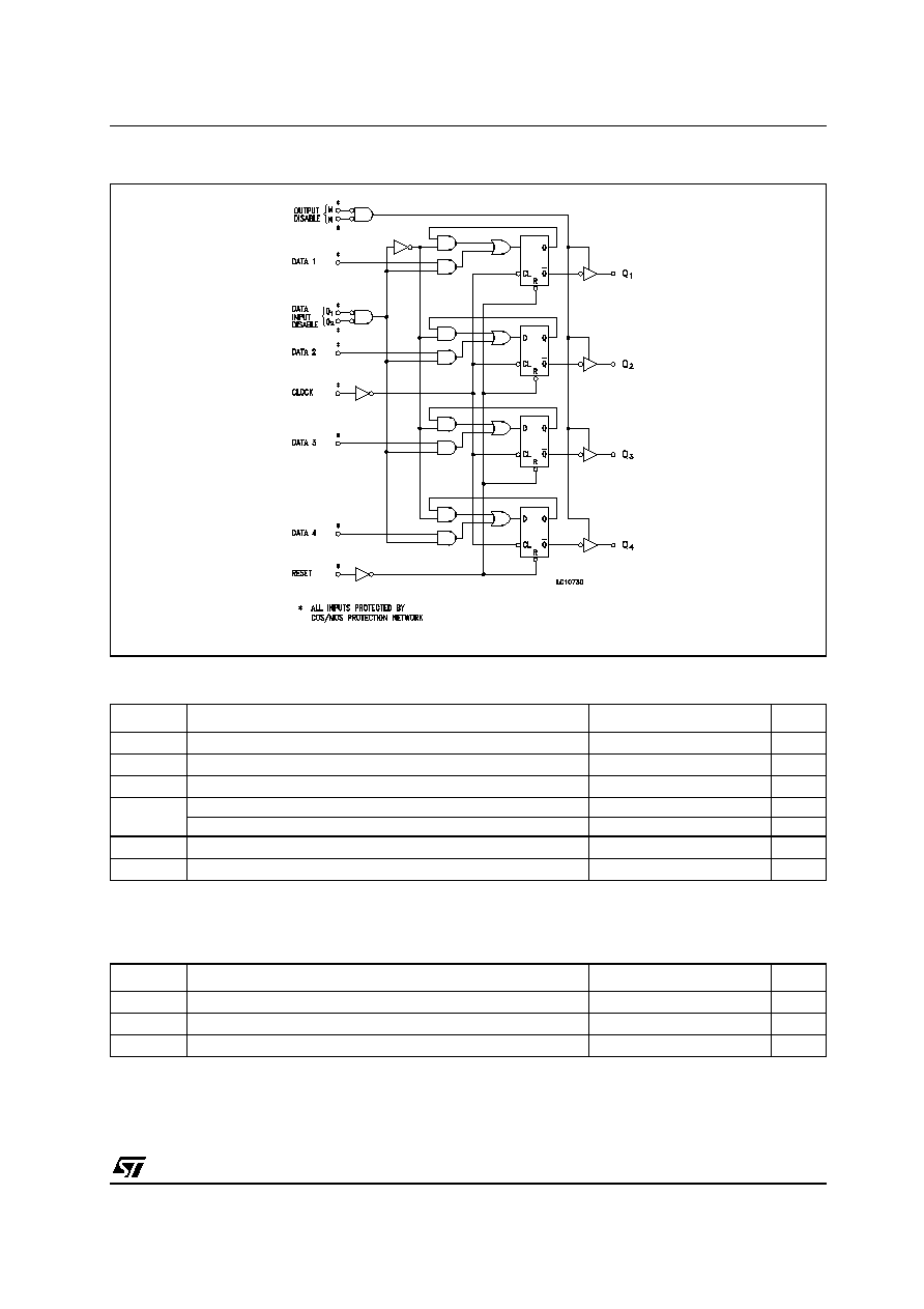
HCF4076B is a monolithic integrated circuit
fabricated in Metal Oxide Semiconductor
technology available in DIP and SOP packages.
HCF4076B is a four bit register consisting of
D-TYPE flip-flops that feature three state outputs.
Data Disable inputs are provided to control the
entry of data into the flip-flops. When both Data
Disable inputs are low, data at the D inputs are
loaded into their respective flip-flops on the next
positive transition of the clock input. Output
Disable inputs are also provided. When the Output
Disable inputs are both low, the normal logic
states of the four outputs are available to the load.
The outputs are disabled independently of the
clock by a high logic level at either Output Disable
input, and present a high impedance.
HCF4076B
4 BIT D TYPE REGISTERS
PIN CONNECTION
ORDER CODES
PACKAGE
TUBE
T & R
DIP
HCF4076BEY
SOP
HCF4076BM1
HCF4076M013TR
DIP
SOP

HCF4076B
2/9
IINPUT EQUIVALENT CIRCUIT
PIN DESCRIPTION
TRUTH TABLE
X : Don't Care
When either Output Disable M or N is high, the outputs are disabled (high impedance state) : however sequential operation of the flip-flop is
not affected.
FUNCTIONAL DIAGRAM
PIN No
SYMBOL
NAME AND FUNCTION
14, 13, 12,
11
DATA1 to
DATA 4
D Inputs
10, 9
G1, G2
Data Input Disable
Control
1, 2
M, N
Output Disable Control
7
CLOCK
Clock Input
15
RESET
Reset Input
8
V
SS
Negative Supply Voltage
16
V
DD
Positive Supply Voltage
RESET
CLOCK
DATA INPUT DISABLE
DATA D
NEXT STATE
OUTPUT
G1
G2
H
X
X
X
X
L
L
L
X
X
X
Q
NO CHANGE
L
H
X
X
Q
NO CHANGE
L
X
H
X
Q
NO CHANGE
L
L
L
H
H
L
L
L
L
L
L
H
X
X
X
Q
NO CHANGE
L
X
X
X
Q
NO CHANGE
HCF4076B
3/9
LOGIC DIAGRAM
ABSOLUTE MAXIMUM RATINGS
Absolute Maximum Ratings are those values beyond which damage to the device may occur. Functional operation under these conditions is
not implied.
All voltage values are referred to V
SS
pin voltage.
RECOMMENDED OPERATING CONDITIONS
Symbol
Parameter
Value
Unit
V
DD
Supply Voltage
-0.5 to +22
V
V
I
DC Input Voltage
-0.5 to V
DD
+ 0.5
V
I
I
DC Input Current
±
10
mA
P
D
Power Dissipation per Package
200
mW
Power Dissipation per Output Transistor
100
mW
T
op
Operating Temperature
-55 to +125
∞C
T
stg
Storage Temperature
-65 to +150
∞C
Symbol
Parameter
Value
Unit
V
DD
Supply Voltage
3 to 20
V
V
I
Input Voltage
0 to V
DD
V
T
op
Operating Temperature
-55 to 125
∞C
HCF4076B
4/9
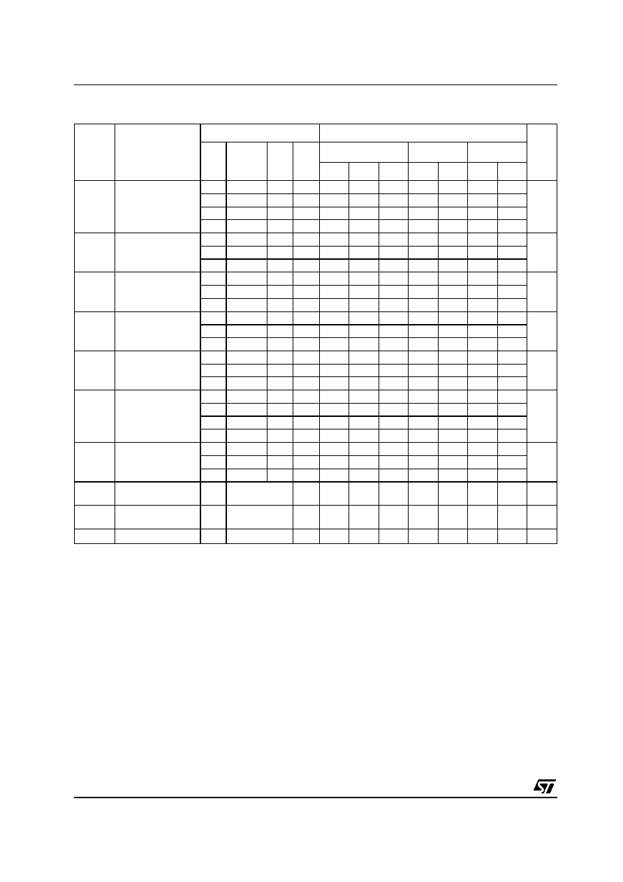
DC SPECIFICATIONS
The Noise Margin for both "1" and "0" level is: 1V min. with V
DD
=5V, 2V min. with V
DD
=10V, 2.5V min. with V
DD
=15V
Symbol
Parameter
Test Condition
Value
Unit
V
I
(V)
V
O
(V)
|I
O
|
(
µ
A)
V
DD
(V)
T
A
= 25∞C
-40 to 85∞C
-55 to 125∞C
Min.
Typ.
Max.
Min.
Max.
Min.
Max.
I
L
Quiescent Current
0/5
5
0.04
5
150
150
µ
A
0/10
10
0.04
10
300
300
0/15
15
0.04
20
600
600
0/20
20
0.08
100
3000
3000
V
OH
High Level Output
Voltage
0/5
<1
5
4.95
4.95
4.95
V
0/10
<1
10
9.95
9.95
9.95
0/15
<1
15
14.95
14.95
14.95
V
OL
Low Level Output
Voltage
5/0
<1
5
0.05
0.05
0.05
V
10/0
<1
10
0.05
0.05
0.05
15/0
<1
15
0.05
0.05
0.05
V
IH
High Level Input
Voltage
0.5/4.5
<1
5
3.5
3.5
3.5
V
1/9
<1
10
7
7
7
1.5/13.5
<1
15
11
11
11
V
IL
Low Level Input
Voltage
4.5/0.5
<1
5
1.5
1.5
1.5
V
9/1
<1
10
3
3
3
13.5/1.5
<1
15
4
4
4
I
OH
Output Drive
Current
0/5
2.5
<1
5
-1.36
-3.2
-1.1
-1.1
mA
0/5
4.6
<1
5
-0.44
-1
-0.36
-0.36
0/10
9.5
<1
10
-1.1
-2.6
-0.9
-0.9
0/15
13.5
<1
15
-3.0
-6.8
-2.4
-2.4
I
OL
Output Sink
Current
0/5
0.4
<1
5
0.44
1
0.36
0.36
mA
0/10
0.5
<1
10
1.1
2.6
0.9
0.9
0/15
1.5
<1
15
3.0
6.8
2.4
2.4
I
I
Input Leakage
Current
0/18
Any Input
18
±
10
-5
±
0.1
±
1
±
1
µ
A
I
OZ
3-State Output
Current
0/18
18
±
10
-4
±
0.4
±
12
±
12
µ
A
C
I
Input Capacitance
Any Input
5
7.5
pF

HCF4076B
5/9
DYNAMIC ELECTRICAL CHARACTERISTICS (T
amb
= 25∞C, C
L
= 50pF, R
L
= 200K
, t
r
= t
f
= 20 ns)
(*) Typical temperature coefficient for all V
DD
value is 0.3 %/∞C.
Symbol
Parameter
Test Condition
Value (*)
Unit
V
DD
(V)
Min.
Typ.
Max.
t
PLH
t
PHL
Propagation Delay Time
(Clock to Q Output)
5
300
600
ns
10
125
250
15
90
180
t
PHL(R)
Propagation Delay Time
(Reset)
5
230
460
ns
10
100
200
15
75
150
t
P(1-H)
3-State Out H or L to High
Impedance
5
R
L
= 1K
150
300
ns
10
75
150
15
60
120
t
P(L-1)
3-State High Impedance to
H or L Output
5
R
L
= 1K
150
300
ns
10
75
150
15
60
120
t
W
Clock Pulse Width
5
200
100
ns
10
100
50
15
80
40
t
W
Reset Pulse Width
5
120
60
ns
10
50
25
15
40
20
t
setup
Data Setup Time
5
200
100
ns
10
80
40
15
60
30
t
setup
Data Input Disable Setup Time
5
180
90
ns
10
100
50
15
70
35
f
max
Maximum Clock Frequency
5
3
6
MHz
10
6
12
15
8
16
t
r,
t
f
Clock input Rise or Fall Time
5
15
µ
s
10
5
15
5