1/11
September 2002
s
CASCADABLE IN MULTIPLES OF 4-BITS
s
SET TO "15" INPUT AND "15" DETECT
OUTPUT
s
QUIESCENT CURRENT SPECIFIED UP TO
20V
s
STANDARDIZED SYMMETRICAL OUTPUT
CHARACTERISTICS
s
5V, 10V AND 15V PARAMETRIC RATINGS
s
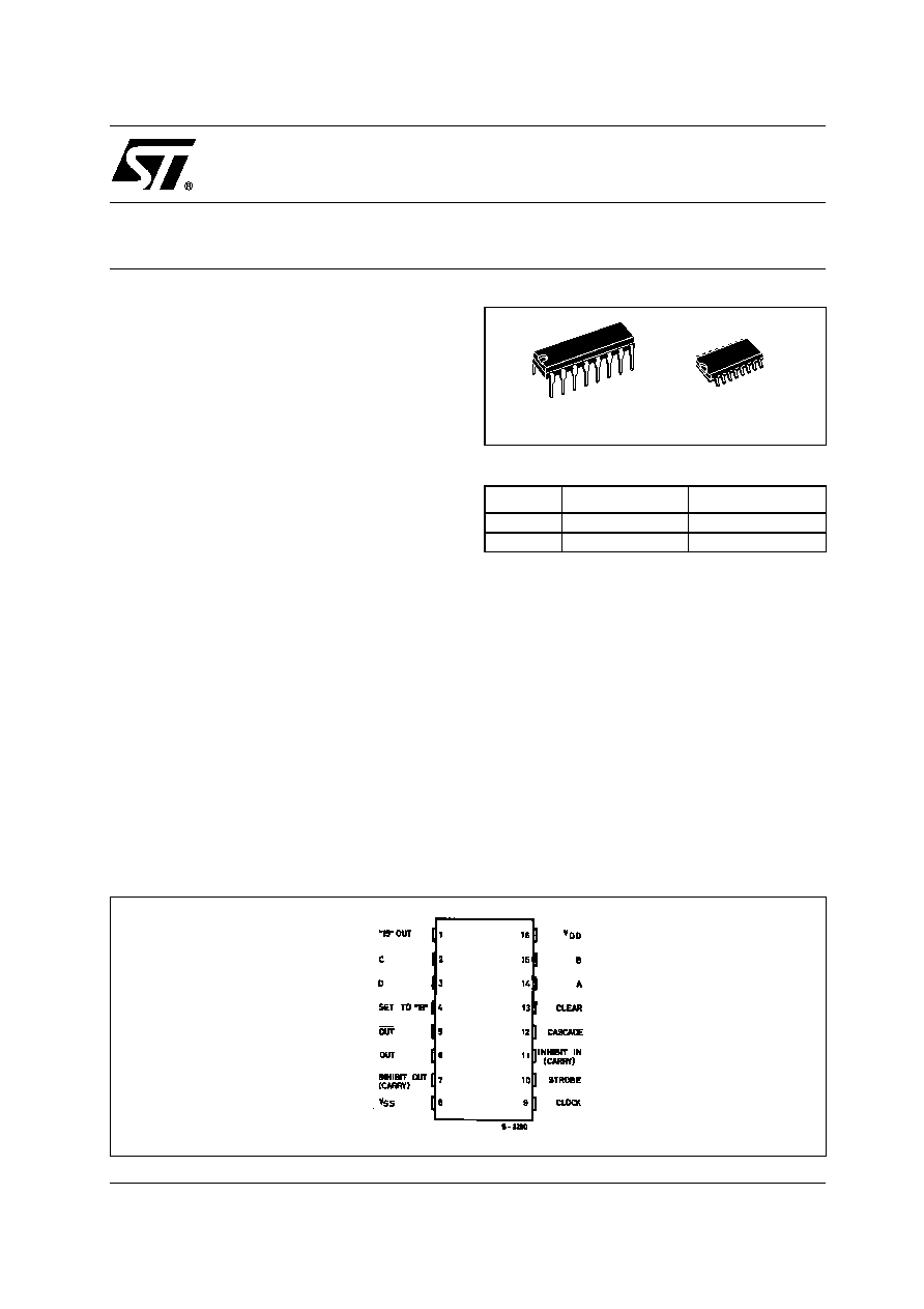
INPUT LEAKAGE CURRENT
I
I
= 100nA (MAX) AT V
DD
= 18V T
A
= 25°C
s
100% TESTED FOR QUIESCENT CURRENT
s
MEETS ALL REQUIREMENTS OF JEDEC
JESD13B "STANDARD SPECIFICATIONS
FOR DESCRIPTION OF B SERIES CMOS
DEVICES"
DESCRIPTION
HCF4089B is a monolithic integrated circuit
fabricated in Metal Oxide Semiconductor
technology available in DIP and SOP packages.
HCF4089B is a low power 4-bit digital rate
multiplier that provides an output pulse rate that is
the clock input pulse rate multiplied by 1/16 times
the binary input. For example, when the binary
input number is 13, ther will be 13 output pulses
for every 16 input pulses.
HCF4089B has an internal synchronous 4-bit
counter, which, together with one of the four
binary inputs bits, produces pulse trains as shown
in the timing diagram.
If more than one binary input bit is high, the
resulting pulse train is a combination of the above
separate pulse trains. This device may be used to
perform arithmetic operations (add, subtract,
divide, raise to a power), solve algebrical and
differential equations, generate natural logarithms
and trigonometric functions, A/D and D/A
conversions, and frequency division.
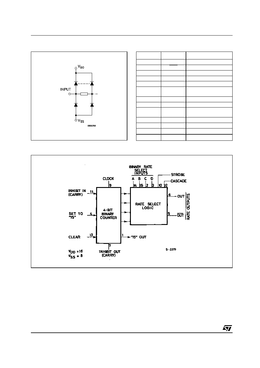
HCF4089B
BINARY RATE MULTIPLIER
PIN CONNECTION
ORDER CODES
PACKAGE
TUBE
T & R
DIP
HCF4089BEY
SOP
HCF4089BM1
HCF4089M013TR
DIP
SOP
HCF4089B
3/11
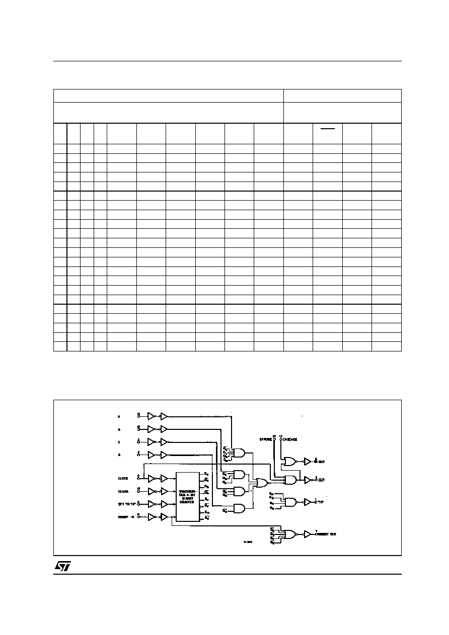
TRUTH TABLE
X : Don't Care
·
:
Depends on internal state of counter
*: Output same as the first 16 lines of this truth table (depending on values of A, B, C, D)
LOGIC DIAGRAM
INPUTS
OUTPUTS
Number of Pulses or Input Logic Level
Number of Pulses or Output Logic
Level
D
C
B
A
CLOCK
INH IN
STR.
CAS.
CLEAR
SET
OUT
OUT
INH
OUT
"15"
OUT
L
L
L
L
16
L
L
L
L
L
L
H
1
1
L
L
L
H
16
L
L
L
L
L
1
1
1
1
L
L
H
L
16
L
L
L
L
L
2
2
1
1
L
L
H
H
16
L
L
L
L
L
3
3
1
1
L
H
L
L
16
L
L
L
L
L
4
4
1
1
L
H
L
H
16
L
L
L
L
L
5
5
1
1
L
H
H
L
16
L
L
L
L
L
6
6
1
1
L
H
H
H
16
L
L
L
L
L
7
7
1
1
H
L
L
L
16
L
L
L
L
L
8
8
1
1
H
L
L
H
16
L
L
L
L
L
9
9
1
1
H
L
H
L
16
L
L
L
L
L
10
10
1
1
H
L
H
H
16
L
L
L
L
L
11
11
1
1
H
H
L
L
16
L
L
L
L
L
12
12
1
1
H
H
L
H
16
L
L
L
L
L
13
13
1
1
H
H
H
L
16
L
L
L
L
L
14
14
1
1
H
H
H
H
16
L
L
L
L
L
15
15
1
1
X
X
X
X
16
H
L
L
L
L
·
·
H
·
X
X
X
X
16
L
H
L
L
L
L
H
1
1
X
X
X
X
16
L
L
H
L
L
H
*
1
1
H
X
X
X
16
L
L
L
H
L
16
16
H
L
L
X
X
X
16
L
L
L
H
L
L
H
H
L
X
X
X
X
16
L
L
L
L
H
L
H
L
H
HCF4089B
4/11
TIMING CHART
ABSOLUTE MAXIMUM RATINGS
Absolute Maximum Ratings are those values beyond which damage to the device may occur. Functional operation under these conditions is
not implied.
All voltage values are referred to V
SS
pin voltage.
RECOMMENDED OPERATING CONDITIONS
Symbol
Parameter
Value
Unit
V
DD
Supply Voltage
-0.5 to +22
V
V
I
DC Input Voltage
-0.5 to V
DD
+ 0.5
V
I
I
DC Input Current
±
10
mA
P
D
Power Dissipation per Package
200
mW
Power Dissipation per Output Transistor
100
mW
T
op
Operating Temperature
-55 to +125
°C
T
stg
Storage Temperature
-65 to +150
°C
Symbol
Parameter
Value
Unit
V
DD
Supply Voltage
3 to 20
V
V
I
Input Voltage
0 to V
DD
V
T
op
Operating Temperature
-55 to 125
°C
HCF4089B
5/11
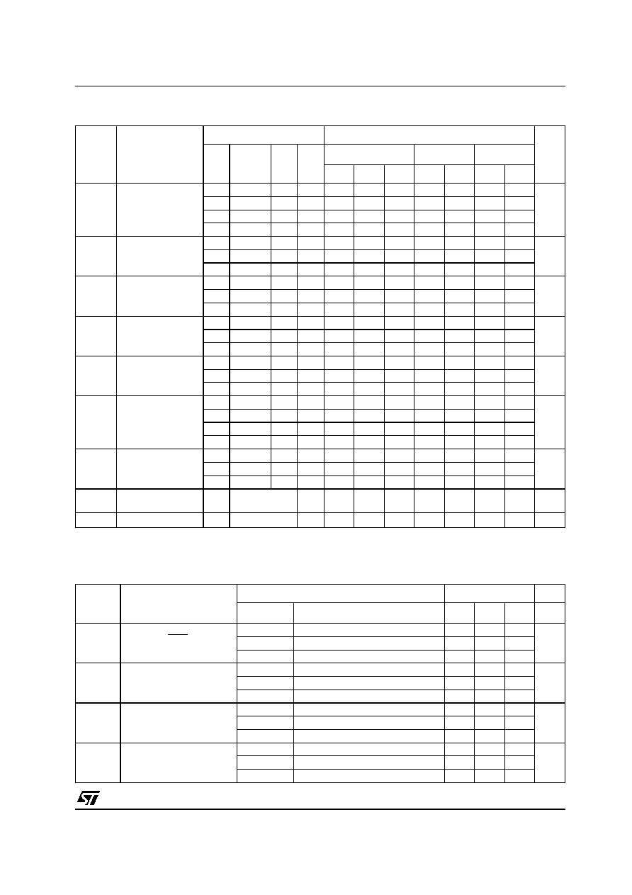
DC SPECIFICATIONS
The Noise Margin for both "1" and "0" level is: 1V min. with V
DD
=5V, 2V min. with V
DD
=10V, 2.5V min. with V
DD
=15V
DYNAMIC ELECTRICAL CHARACTERISTICS (T
amb
= 25°C, C
L
= 50pF, R
L
= 200K
, t
r
= t
f
= 20 ns)
Symbol
Parameter
Test Condition
Value
Unit
V
I
(V)
V
O
(V)
|I
O
|
(
µ
A)
V
DD
(V)
T
A
= 25°C
-40 to 85°C
-55 to 125°C
Min.
Typ.
Max.
Min.
Max.
Min.
Max.
I
L
Quiescent Current
0/5
5
0.04
5
150
150
µ
A
0/10
10
0.04
10
300
300
0/15
15
0.04
20
600
600
0/20
20
0.08
100
3000
3000
V
OH
High Level Output
Voltage
0/5
<1
5
4.95
4.95
4.95
V
0/10
<1
10
9.95
9.95
9.95
0/15
<1
15
14.95
14.95
14.95
V
OL
Low Level Output
Voltage
5/0
<1
5
0.05
0.05
0.05
V
10/0
<1
10
0.05
0.05
0.05
15/0
<1
15
0.05
0.05
0.05
V
IH
High Level Input
Voltage
0.5/4.5
<1
5
3.5
3.5
3.5
V
1/9
<1
10
7
7
7
1.5/13.5
<1
15
11
11
11
V
IL
Low Level Input
Voltage
4.5/0.5
<1
5
1.5
1.5
1.5
V
9/1
<1
10
3
3
3
13.5/1.5
<1
15
4
4
4
I
OH
Output Drive
Current
0/5
2.5
<1
5
-1.36
-3.2
-1.1
-1.1
mA
0/5
4.6
<1
5
-0.44
-1
-0.36
-0.36
0/10
9.5
<1
10
-1.1
-2.6
-0.9
-0.9
0/15
13.5
<1
15
-3.0
-6.8
-2.4
-2.4
I
OL
Output Sink
Current
0/5
0.4
<1
5
0.44
1
0.36
0.36
mA
0/10
0.5
<1
10
1.1
2.6
0.9
0.9
0/15
1.5
<1
15
3.0
6.8
2.4
2.4
I
I
Input Leakage
Current
0/18
Any Input
18
±
10
-5
±
0.1
±
1
±
1
µ
A
C
I
Input Capacitance
Any Input
5
7.5
pF
Symbol
Parameter
Test Condition
Value (*)
Unit
V
DD
(V)
Min.
Typ.
Max.
t
PHL
t
PLH
Propagation Delay Time
CLOCK to OUT
5
110
220
ns
10
55
110
15
45
90
t
PHL
t
PLH
Propagation Delay Time
CLOCK or STROBE to
OUT
5
150
300
ns
10
75
150
15
60
120
t
PHL
t
PLH
Propagation Delay Time
CLOCK to INHIBIT High
Level to Low Level
5
360
720
ns
10
160
320
15
110
220
t
PHL
t
PLH
Propagation Delay Time
LOW Level to HIGH Level
5
250
500
ns
10
100
200
15
75
150