1/7
September 2001
s
SCHMITT TRIGGER ACTION ON EACH
INPUT WITH NO EXTERNAL COMPONENTS
s
HYSTERESIS VOLTAGE TYPICALLY 0.9V at
V
DD
= 5V AND 2.3V at V
DD
= 10V
s
NOISE IMMUNITY GREATER THAN 50%OF
V
DD
(Typ.)
s
NO LIMIT ON INPUT RISE AND FALL TIMES
s
QUIESCENT CURRENT SPECIFIED UP TO
20V
s
STANDARDIZED SYMMETRICAL OUTPUT
CHARACTERISTICS
s
5V, 10V AND 15V PARAMETRIC RATINGS
s
INPUT LEAKAGE CURRENT
I
I
= 100nA (MAX) AT V
DD
= 18V T
A
= 25∞C
s
100% TESTED FOR QUIESCENT CURRENT
s
MEETS ALL REQUIREMENTS OF JEDEC
JESD13B " STANDARD SPECIFICATIONS
FOR DESCRIPTION OF B SERIES CMOS
DEVICES"
DESCRIPTION
The HCF4093B is a monolithic integrated circuit
fabricated in Metal Oxide Semiconductor
technology available in DIP and SOP packages.
The HCF4093B type consists of four schmitt
trigger circuits. Each circuit functions as a two
input NAND gate with schmitt trigger action on
both inputs. The gate switches at different points
for positive and negative going signals. The
difference between the positive voltage (V
P
) and
the negative voltage (V
N
) is defined as hysteresis
voltage (V
H
).
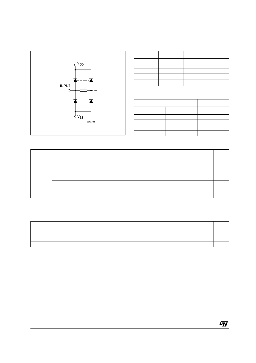
HCF4093B
QUAD 2 INPUT NAND SCHMITT TRIGGER
PIN CONNECTION
ORDER CODES
PACKAGE
TUBE
T & R
DIP
HCF4093BEY
SOP
HCF4093BM1
HCF4093M013TR
DIP
SOP
HCF4093B
2/7
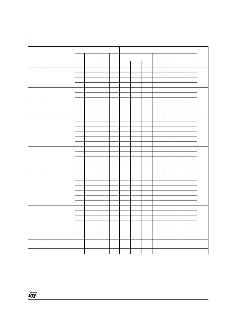
INPUT EQUIVALENT CIRCUIT
PIN DESCRIPTION
TRUTH TABLE
ABSOLUTE MAXIMUM RATINGS
Absolute Maximum Ratings are those values beyond which damage to the device may occur. Functional operation under these conditions is
not implied.
All voltage values are referred to V
SS
pin voltage.
RECOMMENDED OPERATING CONDITIONS
PIN No
SYMBOL
NAME AND FUNCTION
1, 2, 5, 6, 8,
9, 12, 13
A, B, C, D, E,
F, G, H
Data Inputs
3, 4, 10, 11
J, K, L, M
Data Outputs
7
V
SS
Negative Supply Voltage
14
V
DD
Positive Supply Voltage
INPUTS
OUTPUTS
A, C, E, G
B, D, F, H
J, K, L, M
L
L
H
L
H
H
H
L
H
H
H
L
Symbol
Parameter
Value
Unit
V
DD
Supply Voltage
-0.5 to +22
V
V
I
DC Input Voltage
-0.5 to V
DD
+ 0.5
V
I
I
DC Input Current
±
10
mA
P
D
Power Dissipation per Package
200
mW
Power Dissipation per Output Transistor
100
mW
T
op
Operating Temperature
-55 to +125
∞C
T
stg
Storage Temperature
-65 to +150
∞C
Symbol
Parameter
Value
Unit
V
DD
Supply Voltage
3 to 20
V
V
I
Input Voltage
0 to V
DD
V
T
op
Operating Temperature
-55 to 125
∞C
HCF4093B
3/7
DC SPECIFICATIONS
The Noise Margin for both "1" and "0" level is: 1V min. with V
DD
=5V, 2V min. with V
DD
=10V, 2.5V min. with V
DD
=15V
a : Input on terminals 1, 5, 8, 12 or 2, 6, 9, 13; other inputs to V
DD
.
b : Input on terminals 1 and 2, 5 and 6, 8 and 9, or 12 and 13; other inputs to V
DD
.
Symbol
Parameter
Test Condition
Value
Unit
V
I
(V)
V
O
(V)
|I
O
|
(
µ
A)
V
DD
(V)
T
A
= 25∞C
-40 to 85∞C
-55 to 125∞C
Min.
Typ.
Max.
Min.
Max.
Min.
Max.
I
L
Quiescent Current
0/5
5
0.02
1
30
30
µ
A
0/10
10
0.02
2
60
60
0/15
15
0.02
4
120
120
0/20
20
0.04
20
600
600
V
OH
High Level Output
Voltage
0/5
<1
5
4.95
4.95
4.95
V
0/10
<1
10
9.95
9.95
9.95
0/15
<1
15
14.95
14.95
14.95
V
OL
Low Level Output
Voltage
5/0
<1
5
0.05
0.05
0.05
V
10/0
<1
10
0.05
0.05
0.05
15/0
<1
15
0.05
0.05
0.05
V
P
Positive Trigger
Threshold Voltage
a
5
2.2
2.9
3.6
2.2
3.6
2.2
3.6
V
a
10
4.6
5.9
7.1
4.6
7.1
4.6
7.1
a
15
6.8
8.8
10.8
6.8
10.8
6.8
10.8
b
5
2.6
3.3
4.0
2.6
4
2.6
4
b
10
5.6
7
8.2
5.6
8.2
5.6
8.2
b
15
6.3
9.4
12.7
6.3
12.7
6.3
12.7
V
N
Negative Trigger
Threshold Voltage
a
5
0.9
1.9
2.8
0.9
2.8
0.9
2.8
V
a
10
2.5
3.9
5.2
2.5
5.2
2.5
5.2
a
15
4
5.8
7.4
4
7.4
4
7.4
b
5
1.4
2.3
3.2
1.4
3.2
1.4
3.2
b
10
3.4
5.1
6.6
3.4
6.6
3.4
6.6
b
15
4.8
7.3
9.6
4.8
9.6
4.8
9.6
V
H
Hysteresis Voltage
a
5
0.3
0.9
1.6
0.3
1.6
0.3
1.6
V
a
10
1.2
2.3
3.4
1.2
3.4
1.2
3.4
a
15
1.6
3.5
5
1.6
5
1.6
5
b
5
0.3
0.9
1.6
0.3
1.6
0.3
1.6
b
10
1.2
2.3
3.4
1.2
3.4
1.2
3.4
b
15
1.6
3.5
5
1.6
5
1.6
5
I
OH
Output Drive
Current
0/5
2.5
<1
5
-1.36
-3.2
-1.15
-1.1
mA
0/5
4.6
<1
5
-0.44
-1
-0.36
-0.36
0/10
9.5
<1
10
-1.1
-2.6
-0.9
-0.9
0/15
13.5
<1
15
-3.0
-6.8
-2.4
-2.4
I
OL
Output Sink
Current
0/5
0.4
<1
5
0.44
1
0.36
0.36
mA
0/10
0.5
<1
10
1.1
2.6
0.9
0.9
0/15
1.5
<1
15
3.0
6.8
2.4
2.4
I
I
Input Leakage
Current
0/18
Any Input
18
±
10
-5
±
0.1
±
1
±
1
µ
A
C
I
Input Capacitance
Any Input
5
7.5
pF
HCF4093B
4/7
DYNAMIC ELECTRICAL CHARACTERISTICS (T
amb
= 25∞C, C
L
= 50pF, R
L
= 200K
, t
r
= t
f
= 20 ns)
(*) Typical temperature coefficient for all V
DD
value is 0.3 %/∞C.
TEST CIRCUIT
C
L
= 50pF or equivalent (includes jig and probe capacitance)
R
L
= 200K
R
T
= Z
OUT
of pulse generator (typically 50
)
WAVEFORM : PROPAGATION DELAY TIMES (f=1MHz; 50% duty cycle)
Symbol
Parameter
Test Condition
Value (*)
Unit
V
DD
(V)
Min.
Typ.
Max.
t
PLH
t
PHL
Propagation Delay Time
5
190
380
ns
10
90
180
15
65
130
t
TLH
t
THL
Output Transition Time
5
100
200
ns
10
50
100
15
40
80

HCF4093B
5/7
DIM.
mm.
inch
MIN.
TYP
MAX.
MIN.
TYP.
MAX.
a1
0.51
0.020
B
1.39
1.65
0.055
0.065
b
0.5
0.020
b1
0.25
0.010
D
20
0.787
E
8.5
0.335
e
2.54
0.100
e3
15.24
0.600
F
7.1
0.280
I
5.1
0.201
L
3.3
0.130
Z
1.27
2.54
0.050
0.100
Plastic DIP-14 MECHANICAL DATA
P001A

HCF4093B
6/7
DIM.
mm.
inch
MIN.
TYP
MAX.
MIN.
TYP.
MAX.
A
1.75
0.068
a1
0.1
0.2
0.003
0.007
a2
1.65
0.064
b
0.35
0.46
0.013
0.018
b1
0.19
0.25
0.007
0.010
C
0.5
0.019
c1
45∞ (typ.)
D
8.55
8.75
0.336
0.344
E
5.8
6.2
0.228
0.244
e
1.27
0.050
e3
7.62
0.300
F
3.8
4.0
0.149
0.157
G
4.6
5.3
0.181
0.208
L
0.5
1.27
0.019
0.050
M
0.68
0.026
S
8∞ (max.)
SO-14 MECHANICAL DATA
PO13G

HCF4093B
Information furnished is believed to be accurate and reliable. However, STMicroelectronics assumes no responsibility for the
consequences of use of such information nor for any infringement of patents or other rights of third parties which may result from
its use. No license is granted by implication or otherwise under any patent or patent rights of STMicroelectronics. Specifications
mentioned in this publication are subject to change without notice. This publication supersedes and replaces all information
previously supplied. STMicroelectronics products are not authorized for use as critical components in life support devices or
systems without express written approval of STMicroelectronics.
© The ST logo is a registered trademark of STMicroelectronics
© 2001 STMicroelectronics - Printed in Italy - All Rights Reserved
STMicroelectronics GROUP OF COMPANIES
Australia - Brazil - China - Finland - France - Germany - Hong Kong - India - Italy - Japan - Malaysia - Malta - Morocco
Singapore - Spain - Sweden - Switzerland - United Kingdom
© http://www.st.com
7/7