HCC/HCF4067B
HCC/HCF4097B
September 1988
ANALOG MULTIPLEXER/DEMULTIPLEXER
EY
(Plastic Package)
ORDER CODES :
HCC40XXBF
HCF40XXBM1
HCF40XXBEY
HCF40XXBC1
F
(Ceramic Package)
M1
(Micro Package)
C1
(Chip Carrier)
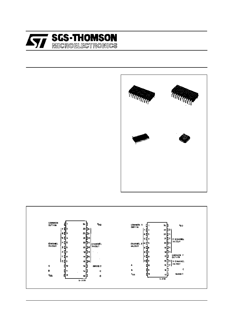
PIN CONNECTIONS
.
LOW ON RESISTANCE: 125
(typ.) OVER 15
Vp-p SIGNAL INPUT RANGE FOR
V
DD
- V
SS
= 15V
.
HIGH OFF RESISTANCE: CHANNEL LEAK-
AGE OF
±
10pA (typ.) @ V
DD
- V
SS
= 10V
.
MATCHED
SWITCH
CHARACTERISTICS:
R
ON
= 5
(typ.) FOR V
DD
- V
SS
= 15V
.
VERY LOW QUIESCENT POWER DISSIPA-
TION UNDER A DIGITAL CONTROL INPUT
AND SUPPLY CONDITIONS: 0.2
µ
W (typ.) @
V
DD
-V
SS
= 10V
.
BINARY ADDRESS DECODING ON CHIP
.
QUIESCENT CURRENT SPECIFIED TO 20V
FOR HCC DEVICE
.
STANDARDIZED
SYMMETRICAL
OUTPUT
CHARACTERISTICS
.
5V, 10V AND 15V PARAMETRIC RATINGS
.
INPUT CURRENT OF 100nA AT 18V AND 25
o
C
FOR HCC DEVICE
.
100% TESTED FOR QUIESCENT CURRENT
.
MEETS ALL REQUIREMENTS OF JEDEC TEN-
TATIVE STANDARD No 13A, "STANDARD
SPECIFICATIONS FOR DESCRIPTION OF B
SERIE CMOS DEVICES"
4067B
4097B
4067B≠SINGLE 16-CHANNEL
4097B≠DIFFERENTIAL 8-CHANNEL
1/16

DESCRIPTION
The HCC4067B, HCC4097B (extended tempera-
ture range) and HCF4067B, HCF4097B (intermedi-
ate temperature range) are monolithic integrated
circuits available in 24-lead dual in line plastic or ce-
ramic package.
The
HCC/HCF4067B
and
HCC/HCF4097B
COS/MOS analog multiplexers/demultiplexers are
digitally controlled analog switches having low ON
impedance, low OFF leakage current and internal
address decoding. in addition, the ON resistance is
relatively constant over the full input-signal range.
The HCC/HCF4067B ia a 16-channel multiplexer
with four binary control inputs A, B, C, D, and an in-
hibit input, arranged so that any combination of the
inputs selects one switch.
The HCC/HCF4097 is a differential 8-channel multi-
plexer having three binary control inputs A, B, C, and
an inhibit input. The inputs permit selection of one
FUNCTIONAL DIAGRAM
For 4067B
For 4097B
HCC/HCF4067B HCC/HCF4097B
2/16

LOGIC DIAGRAM
For 4067B
HCC/HCF4067B HCC/HCF4097B
3/16
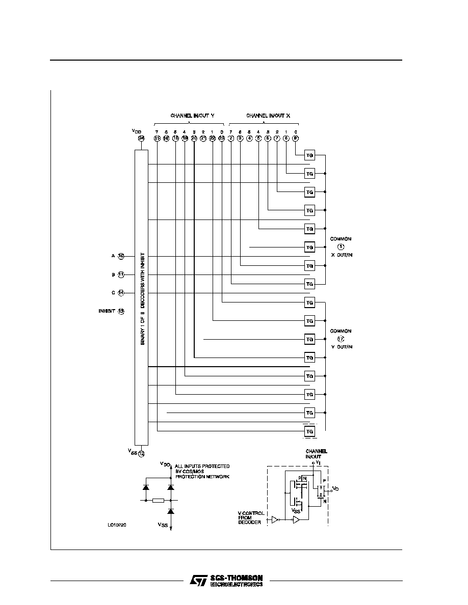
LOGIC DIAGRAM
For 4097B
HCC/HCF4067B HCC/HCF4097B
4/16

ABSOLUTE MAXIMUM RATING
Symbol
Parameter
Value
Unit
V
DD
*
Supply Voltage: HCC Types
HCF Types
-0.5 to +20
-0.5 to +18
V
V
V
i
Input Voltage
-0.5 to V
DD
+ 0.5
V
I
I
DC Input Current (any one input)
±
10
mA
P
tot
Total Power Dissipation (per package)
Dissipation per Output Transistor
for Top = Full Package Temperature Range
200
100
mW
mW
T
op
Operating Temperature: HCC Types
HCF Types
-55 to +125
-40 to +85
o
C
o
C
T
stg
Storage Temperature
-65 to +150
o
C
Stresses above those listed under "Absolute Maximum Ratings" may cause permanent damage to the device. This is a stress ratingonly and functional
operation of the device at these or any other conditions above those indicated in the operational sections of this specification is not implied. Exposure
to absolute maximum rating conditions for external periods may affect device reliability.
* All voltage values are referred to V
SS
pin voltage.
RECOMMENDED OPERATING CONDITIONS
Symbol
Parameter
Value
Unit
V
DD
Supply Voltage: HCC Types
HCF Types
3 to 18
3 to 15
V
V
V
I
Input Voltage
0 to V
DD
V
T
op
Operating Temperature: HCC Types
HCF Types
-55 to +125
-40 to +85
o
C
o
C
TRUTH TABLES FOR HCC/HCF4067B
A
B
C
D
INH
SELECTED
CHANNEL
X
X
X
X
1
None
0
0
0
0
0
0
1
0
0
0
0
1
0
1
0
0
0
2
1
1
0
0
0
3
0
0
1
0
0
4
1
0
1
0
0
5
0
1
1
0
0
6
1
1
1
0
0
7
0
0
0
1
0
8
1
0
0
1
0
9
0
1
0
1
0
10
1
1
0
1
0
11
0
0
1
1
0
12
1
0
1
1
0
13
0
1
1
1
0
14
1
1
1
1
0
15
TRUTH TABLE FOR HCC/HCF4097B
A
B
C
INH
SELECTED
CHANNEL
X
X
X
1
None
0
0
0
0
0X 0Y
1
0
0
0
1X 1Y
0
1
0
0
2X 2Y
1
1
0
0
3X 3Y
0
0
1
0
4X 4Y
1
0
1
0
5X 5Y
0
1
1
0
6X 6Y
1
1
1
0
7X 7Y
HCC/HCF4067B HCC/HCF4097B
5/16
STATIC ELECTRICAL CHARACTERISTICS (over recommended operating conditions)
Symbol
Parameter
Test Conditios
Value
Unit
V
IS
(V)
V
EE
(V)
V
SS
(V)
V
DD
(V)
T
LOW
*
25
o
C
T
HIGH
*
Min.
Max.
Min.
Typ.
Max.
Min.
Max.
I
L
Quiescent
Supply
Current
HCC
types
5
5
0.04
5
150
µ
A
10
10
0.04
10
300
15
20
0.04
20
600
20
100
0.08
100
3000
HCF
types
5
20
0.04
20
150
10
40
0.04
40
300
15
80
0.04
80
600
SWITCH
R
ON
On
Resistance
HCC
types
0
V
I
V
DD
0
0
5
800
470
1050
1300
10
310
180
400
580
15
200
125
240
320
HCF
types
0
V
I
V
DD
0
0
5
850
470
1050
1200
10
330
180
400
520
15
210
125
240
300
ON
Resistance
R
ON
(Between any two
channels)
0
0
5
10
10
10
15
5
OFF (
∑
)
Channel
Leakage
Current
Any
Channel OFF
HCC
types
0
0
18
100
±
0.1
100
1000
µ
A
All Channel
OFF
(common
OUT/IN)
HCC
types
0
0
18
100
±
0.1
100
1000
Any
Channel OFF
HCF
types
0
0
15
300
±
0.1
300
1000
All Channel
OFF
(common
OUT/IN)
HCF
types
0
0
15
300
±
0.1
300
1000
C
Capacitance
Input
Output for 4067
Output for 4097
Feedthrough
-5
5
5
55
35
0.2
pF
CONTROL
V
IL
Input Low
Voltage
= V
DD
thru
1K
V
EE
=V
SS
R
L
=1K
to V
SS
I
IS
< 2
µ
A
(on all OFF
channels)
5
1.5
1.5
1.5
V
10
3
3
3
15
4
4
4
V
IH
Input High
Voltage
5
3.5
3.5
3.5
V
10
7
7
7
15
11
11
11
I
IH
I
IL
Input
Leackage
Current
HCC
types
V
I
= 0/18V
18
±
0.1
±
10
-3
±
0.1
±
1
µ
A
HCF
types
V
I
= 0/15V
15
±
0.3
±
10
-3
±
0.3
±
1
C
I
Input Capacitance
Any Address or
Inhibit Input
5
7.5
pF
∑
Determined by minimum feasible leakage measurement for automatic testing
* T
LOW
= -55
o
C for HCC device: -40
o
C for HCF device.
* T
HIGH
= +125
o
C for HCC device: +85
o
C for HCF device.
The Noise Margin for both "1" and "0" level is: 1V min. with V
DD
= 5 V, 2 V min. with V
DD
= 10 V, 2.5 V min. with V
DD
= 15 V
HCC/HCF4067B HCC/HCF4097B
6/16

DYNAMIC ELECTRICAL CHARACTERISTICS (T
amb
= 25
o
C, C
L
= 50 pF, R
L
= 200 K
,
typical temperature coefficent for all V
DD
values is 03 %/
o
C, all input rise and fall times= 20 ns)
Symbol
Parameter
Test Conditions
Value
Unit
V
C
(V)
R
L
(K
)
f
i
(KHz)
V
I
(V)
V
SS
(V)
V
DD
(V)
Typ. Max.
SWITCH
t
pd
Propagation Delay
Time (Signal Input to
Output)
= V
DD
200
0
5
30
60
ns
10
15
30
15
11
20
Frequency Response
Channel "ON" (Sine
Wave Input) at
20
Log
V
O
V
I
= -
3
dB
= V
DD
1
5 (
∑
)
0
10
V
O
at
Common
OUT/IN
4067B
14
ns
4097B
20
V
O
at Any Channel
60
Feedthrough (All
Channels OFF) at
20
Log
V
O
V
I
= -
40
dB
= V
SS
1
5 (
∑
)
0
10
V
O
at
Common
OUT/IN
4067B
20
MHz
4097B
12
V
O
at Any Channel
8
Frequency Signal
Crosstalk at
20
Log
V
O
(
B
)
V
I
(
A
)
= -
40
dB
V
C(A)
=V
DD
V
C(B)
=V
SS
1
5 (
∑
)
0
10
Between Any two (A
and B) Channels
1
MHz
Between
Sections
(A and B)
4097B
only
Measured
on
common
10
Measured
on Any
Channel
18
t
W
Sine Wave Distortion
(f
is
= 1KHz sine
wave)
5
10
1
2 (
∑
)
0
5
0.3
%
10
10
1
3 (
∑
)
0
10
0.2
15
10
1
5 (
∑
)
0
15
0.12
CONTROL (address or Inhibit)
t
PLH
t
PHL
Propagation Delay
Time: Address or
Inhibit to Signal OUT
(Channel Turning ON)
1
0
5
325
650
ns
0
10
135
270
0
15
95
190
t
PLH
t
PHL
Propagation Delay
Time: Address or
Inhibit to Signal OUT
(Channel Turning
OFF)
0.3
0
5
220
440
ns
0
10
90
180
0
15
65
130
Address or Inhibit to
Signal Crosstalk
10*
0
10
75
mV
peak
(
∑
) Peak to peak voltage symmetrical about
V
DD
-
V
SS
2
(*) Both ends of channel
HCC/HCF4067B HCC/HCF4097B
7/16
Typical ON Resistance vs Input Signal Voltage
(All Types)
Typical ON Resistance vs Input Signal Voltage
(All Types)
TEST CIRCUITS
Typical ON Resistance vs Input Signal Voltage
(All Types)
Typical ON Resistance vs Input Signal Voltage
(All Types)
OFF Channel Leakage Current Any Channel OFF
For 4067B
For 4097B
HCC/HCF4067B HCC/HCF4097B
8/16
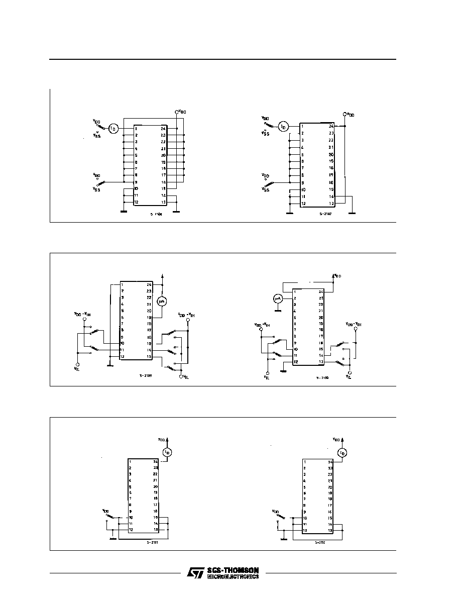
Quiescent Device Current
For 4067B
For 4097B
Input Voltage Measure < 2
µ
A an All OFF Channels (e.g. Channel 12)
OFF Channel Leakage Current All Channels OFF
For 4067B
For 4097B
For 4097B
For 4067B
HCC/HCF4067B HCC/HCF4097B
9/16

Channel ON Resistance Measurement Circuit
Turn-on and Turn-off Propagation Delay-Inhibit Input to Signal Output (e. g. Channel 1)
Turn-on and Turn-off Propagation Delay Address Select Input to Signal Output (e. g. Channel 0)
For 4067B
For 4097B
For 4097B
For 4067B
HCC/HCF4067B HCC/HCF4097B
10/16
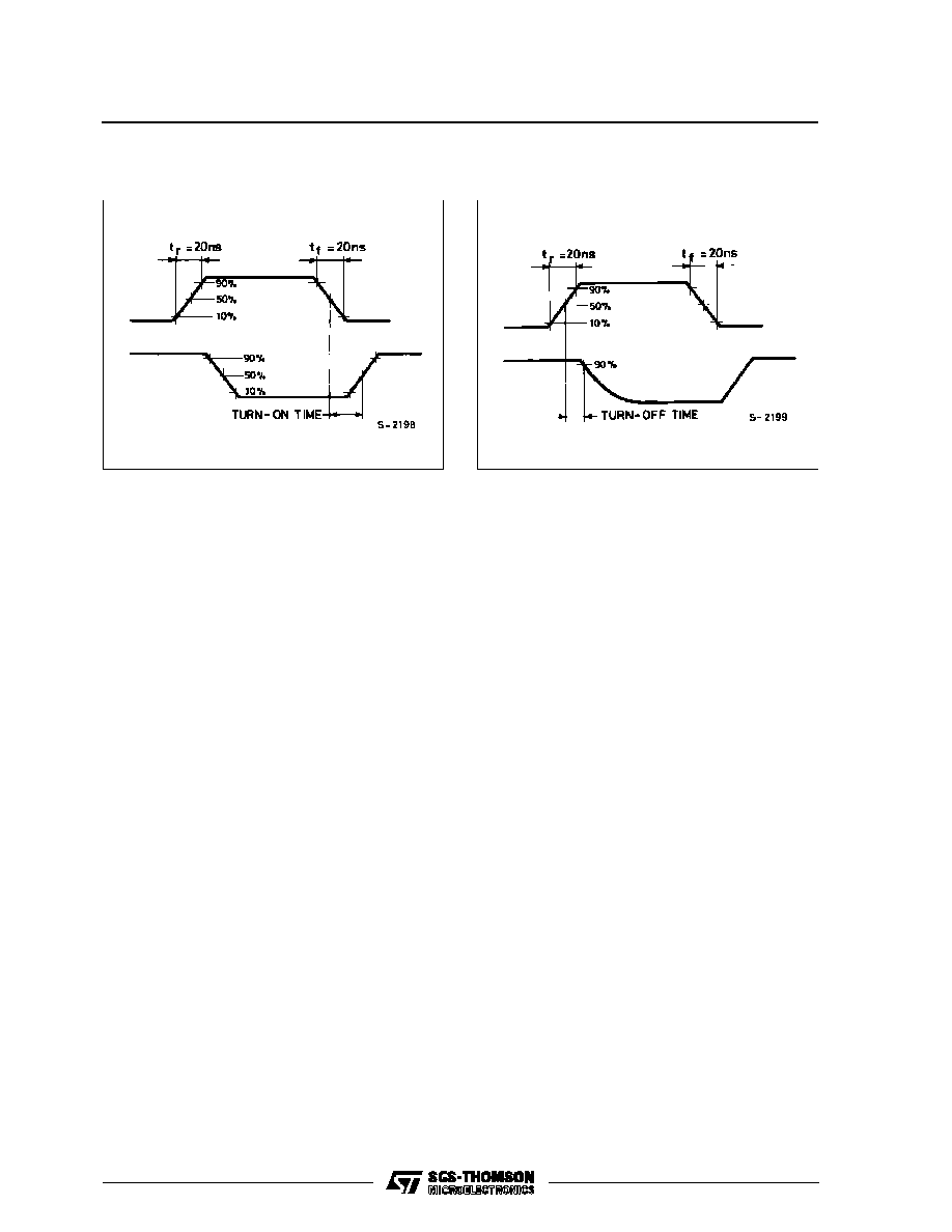
Propagation Delay Waveform Channel Being
Turned ON (R
L
= 10 K
, C
L
= 50 pF)
Propagation Delay Waveform Channel Being
Turned OFF (R
L
= 300
, C
L
= 50 pF)
APPLICATIONS INFORMATION
In applications where separate power sources are
used to drive V
DD
and the signal inputs, the V
DD
cur-
rent capability should exceed V
DD
/R
L
(R
L
= effective
external load). This provision avoids permanent cur-
rent flow or clamp action on the V
DD
supply when
power
is
applied
or
removed
from
the
HCC/HCF4067B or HCC/HCF4097B.
When switching from one address to another, some
of the ON periods of the channels of the multiplexers
will overlap momentarily, which may be objection-
able in certain applications. Also when a channel is
turned ON or OFF by an address input, there is a
momentary conductive path from the channel to
VSS, which will drump some charge from any capa-
citor connected to the input or output of the channel.
The inhibit input turning on a channel will similarly
drump some charge to V
SS
.
The amount of charge dumped is mostly a function
of the signal level above V
SS
.
Typically, ay V
DD
- V
SS
= 10V, a 100 pF capacitor
connected to the input or output of the channel will
lose 3-4% of its voltage at the moment the channel
turns ON or OFF. This loss of voltage is essentially
independent of the address or inhibit signal trnasi-
tion time, if the transition time is less than 1- 2
µ
s.
When the inhibit signal turns a channel off, there is
no change dumping of V
SS
. Rather, there is a slight
rise in the channel voltage level (65 mV typ.) due to
the capacitance coupling from inhibit input to chan-
nel input or output. Address input also couple some
voltage steps onto the channel signal levels.
In certain applications, the external load-resistor
current may include both V
DD
and signal line com-
ponents. To avoid drawing V
DD
current when switch
current flows into the transmission gate inputs, the
voltage drop across the bidirectional switch must not
exceed 0.8 V (calculated from R
ON
values shown in
ELECTRICAL CHARACTERISTICS CHART). No
VDD current will flow through R
L
if the switch current
flows into terminal 1 on the HCC/HCF4067B, termi-
nals 1 and 17 on the HCC/HCF4097B.
HCC/HCF4067B HCC/HCF4097B
11/16
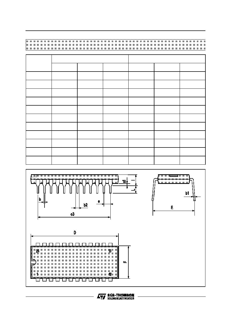
Plastic DIP24 (0.25) MECHANICAL DATA
DIM.
mm
inch
MIN.
TYP.
MAX.
MIN.
TYP.
MAX.
a1
0.63
0.025
b
0.45
0.018
b1
0.23
0.31
0.009
0.012
b2
1.27
0.050
D
32.2
1.268
E
15.2
16.68
0.598
0.657
e
2.54
0.100
e3
27.94
1.100
F
14.1
0.555
I
4.445
0.175
L
3.3
0.130
P043A
HCC/HCF4067B HCC/HCF4097B
12/16
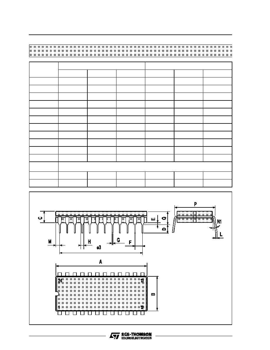
Ceramic DIP24 MECHANICAL DATA
DIM.
mm
inch
MIN.
TYP.
MAX.
MIN.
TYP.
MAX.
A
32.3
1.272
B
13.05
13.36
0.514
0.526
C
3.9
5.08
0.154
0.200
D
3
0.118
E
0.5
1.78
0.020
0.070
e3
27.94
1.100
F
2.29
2.79
0.090
0.110
G
0.4
0.55
0.016
0.022
I
1.17
1.52
0.046
0.060
L
0.22
0.31
0.009
0.012
M
1.52
2.49
0.060
0.098
N1
4
∞
(min.), 15
∞
(max.)
P
15.4
15.8
0.606
0.622
Q
5.71
0.225
P058C
HCC/HCF4067B HCC/HCF4097B
13/16

SO24 MECHANICAL DATA
DIM.
mm
inch
MIN.
TYP.
MAX.
MIN.
TYP.
MAX.
A
2.65
0.104
a1
0.10
0.20
0.004
0.007
a2
2.45
0.096
b
0.35
0.49
0.013
0.019
b1
0.23
0.32
0.009
0.012
C
0.50
0.020
c1
45
∞
(typ.)
D
15.20
15.60
0.598
0.614
E
10.00
10.65
0.393
0.420
e
1.27
0.05
e3
13.97
0.55
F
7.40
7.60
0.291
0.299
L
0.50
1.27
0.19
0.050
S
8
∞
(max.)
F
C
L
E
a1
b1
A
e
D
e3
b
24
13
1
12
c1
s
a2
HCC/HCF4067B HCC/HCF4097B
14/16
PLCC20 MECHANICAL DATA
DIM.
mm
inch
MIN.
TYP.
MAX.
MIN.
TYP.
MAX.
A
9.78
10.03
0.385
0.395
B
8.89
9.04
0.350
0.356
D
4.2
4.57
0.165
0.180
d1
2.54
0.100
d2
0.56
0.022
E
7.37
8.38
0.290
0.330
e
1.27
0.050
e3
5.08
0.200
F
0.38
0.015
G
0.101
0.004
M
1.27
0.050
M1
1.14
0.045
P027A
HCC/HCF4067B HCC/HCF4097B
15/16
Information furnished is believed to be accurate and reliable. However, SGS-THOMSON Microelectronics assumes no responsability for the
consequences of use of such information nor for any infringement of patents or other rights of third parties which may results from its use. No
license is granted by implication or otherwise under any patent or patent rights of SGS-THOMSON Microelectronics. Specifications mentioned
in this publication are subject to change without notice. This publication supersedes and replaces all information previously supplied.
SGS-THOMSON Microelectronics products are not authorized for use as critical components in life support devices or systems without express
written approval of SGS-THOMSON Microelectonics.
©
1994 SGS-THOMSON Microelectronics - All Rights Reserved
SGS-THOMSON Microelectronics GROUP OF COMPANIES
Australia - Brazil - France - Germany - Hong Kong - Italy - Japan - Korea - Malaysia - Malta - Morocco - The Netherlands -
Singapore - Spain - Sweden - Switzerland - Taiwan - Thailand - United Kingdom - U.S.A
HCC/HCF4067B HCC/HCF4097B
16/16