 | –≠–ª–µ–∫—Ç—Ä–æ–Ω–Ω—ã–π –∫–æ–º–ø–æ–Ω–µ–Ω—Ç: HCF4510 | –°–∫–∞—á–∞—Ç—å:  PDF PDF  ZIP ZIP |
HCF4510B
HCF4516B
PRESETTABLE UP/DOWN COUNTERS
March 2000
s
MEDIUM SPEED OPERATION f
CL
= 8MHz
TYP. AT 10V
s
SYNCHRONOUS INTERNAL CARRY
PROPAGATION
s
RESET AND PRESET CAPABILITY
s
QUIESCENT CURRENT SPECIFIED TO 15V
s
5V, 10V, AND 15V PARAMETRIC RATINGS
s
INPUT CURRENT OF 100nAAT 15V AND 25
∞
C
s
100% TESTED FOR QUIESCENT CURRENT
MEETS
ALL
REQUIREMENTS
OF
JEDEC
TENTATIVE STANDARD No. 13A, "STANDARD
SPECIFICATIONS FOR DESCRIPTION OF "B"
SERIES CMOS DEVICES"
DESCRIPTION
The HCF4510B and HCF4516B are monolithic
integrated circuits available in 16-lead dual in-line
plastic
and
plastic
micro
package.
The
HCF4510B Presettable BCD Up/Down Counter
and the HCF4516B Presettable Binary Up/Down
Counter consist of four synchronously clocked
D-type flip-flops (with a gating structure to provide
T-type flip-flop capability) connected as counters.
These counters can be cleared by a high level on
the RESET line, and can be preset to any binary
number present on the jam inputs by a high level
on the PRESET ENABLE line. The HCF4510B
will count out of non-BCD counter states in a
maximum of two clock pulses in the up mode,
and a maximum of four clock pulses in the down
mode. If the CARRY-IN input is held low, the
counter
advances
up
or
down
on
each
positive-going
clock
transition.
Synchronous
cascading is accomplished by connecting all
clock inputs in parallel and connecting the
CARRY-OUT of a less significant stage to the
CARRY-IN of a more significant stage. The
HCF4510B and HCF4516B can be loaded in the
ripple mode by connecting the CARRY-OUT to
the clock of the next stage. If the UP/DOWN input
changes
during
a
terminal
count,
the
CARRY-OUT must be gated with the clock, and
the UP/DOWN input must change while the clock
is high. This method provides a clean clock signal
to the subsequent counting stage.
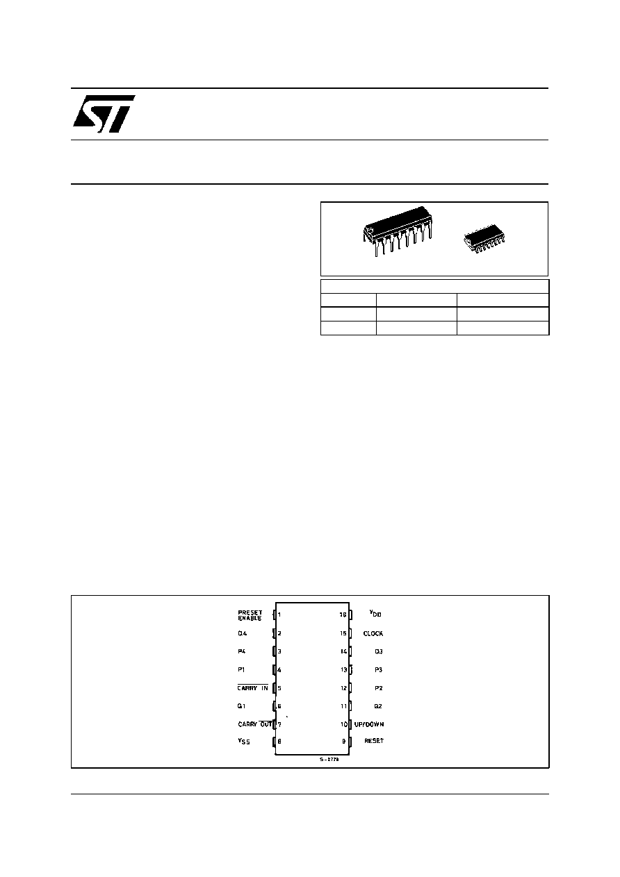
PIN CONNECTION
Æ
SOP
DIP
ORDER CODES
PACKAGE
TUBE
T & R
DIP
HCF45XXBEY
SOP
HCF45XXBM1
HCF45XXM013TR
1/12

FUNCTIONAL DIAGRAM
ABSOLUTE MAXIMUM RATING
Symbol
Parameter
Val ue
Unit
V
DD
*
Supply Voltage
-0.5 to +18
V
V
i
Input Voltage
-0.5 to V
DD
+ 0.5
V
I
I
DC Input Current (any one input)
±
10
mA
P
tot
Total Power Dissipation (per package)
Dissipation per Output Transistor
for Top = Full Package Temperature Range
200
100
mW
mW
T
op
Operating Temperature
-40 to +85
o
C
T
stg
Storage Temperature
-65 to +150
o
C
Stresses above those listedunder "Absolute Maximum Ratings" may cause permanent damage to the device. This is a stress rating only and functional
operation ofthe device atthese or any other conditions above those indicated in the operational sections of this specification is not implied. Exposure to
absolute maximum ratingconditions for external periods may affect device reliability.
* Allvoltage values are referred to V
SS
pin voltage.
RECOMMENDED OPERATING CONDITIONS
Symbol
Parameter
Val ue
Unit
V
DD
Supply Voltage
3 to 15
V
V
I
Input Voltage
0 to V
DD
V
T
op
Operating Temperature
-40 to +85
o
C
TRUTH TABLE
CL
CI
U/D
PE
R
Actio n
X
1
X
0
0
No Count
0
1
0
0
Count Up
0
0
0
0
Count Down
X
X
X
1
0
Preset
X
X
X
X
1
Reset
X= Don't care
HCF4510B/4515B
2/12
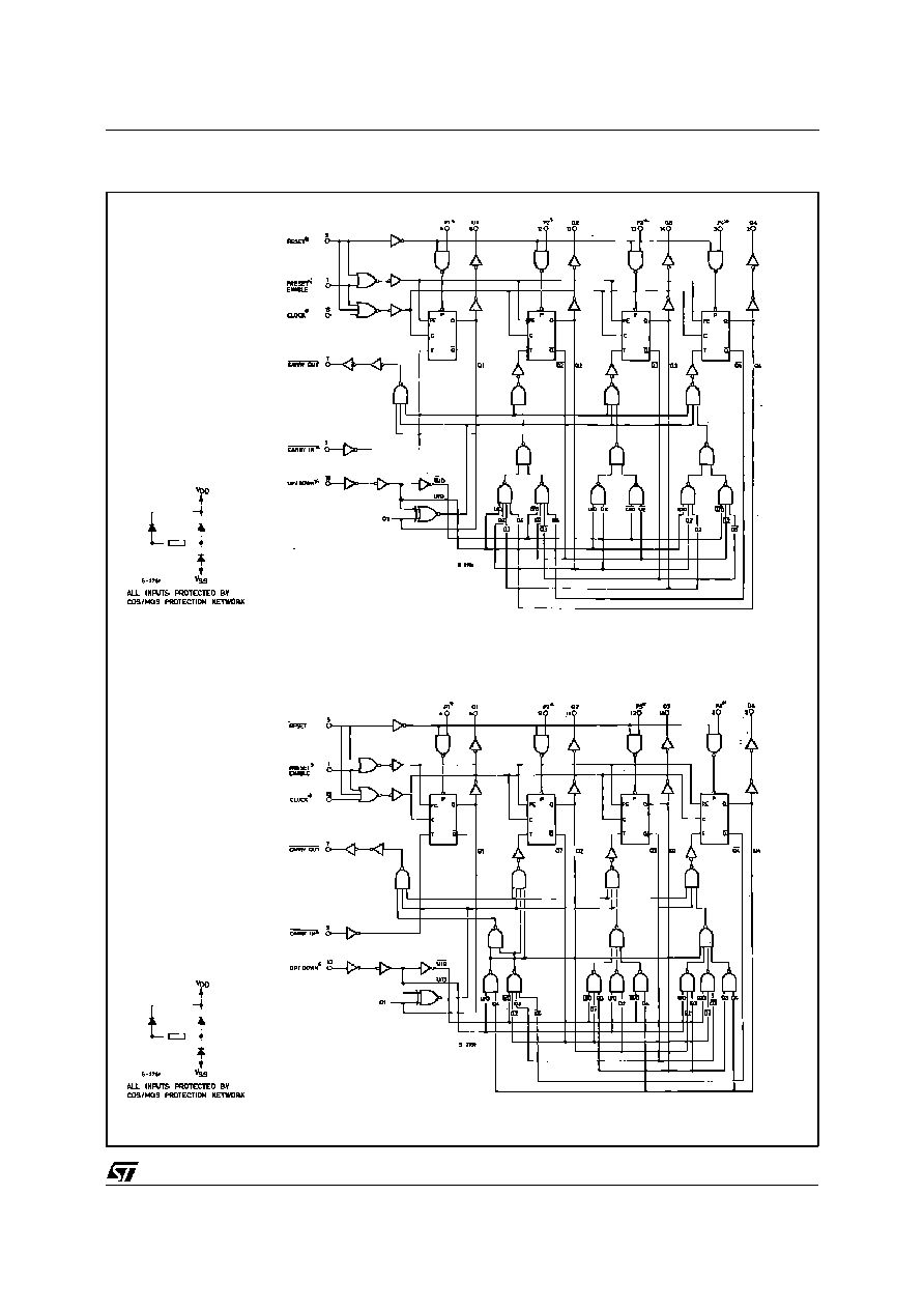
LOGIC DIAGRAMS
4510B
4516B
HCF4510B/4516B
3/12

TIMING DIAGRAMS
4510B
4516B
HCF4510B/4515B
4/12
STATIC ELECTRICAL CHARACTERISTICS (over recommended operating conditions)
Symb ol
Parameter
T est Cond it ios
Valu e
Un it
V
I
(V)
V
O
(V)
| I
O
|
(
µ
A)
V
DD
(V)
-40
o
C
25
o
C
85
o
C
Mi n. Max. Min. T yp. Max. Min . Max.
I
L
Quiescent Current
0/5
5
20
0.02
20
150
µ
A
0/10
10
40
0.02
40
300
0/15
15
80
0.02
80
600
V
OH
Output High
Voltage
0/5
< 1
5
4.95
4.95
4.95
V
0/10
< 1
10
9.95
9.95
9.95
0/15
< 1
15
14.95
14.95
14.95
V
OL
Output Low
Voltage
5/0
< 1
5
0.05
0.05
0.05
V
10/0
< 1
10
0.05
0.05
0.05
15/0
< 1
15
0.05
0.05
0.05
V
IH
Input High
Voltage
0.5/4.5
< 1
5
3.5
3.5
3.5
V
1/9
< 1
10
7
7
7
1.5/13.5
< 1
15
11
11
11
V
IL
Input Low
Voltage
4.5/0.5
< 1
5
1.5
1.5
1.5
V
9/1
< 1
10
3
3
3
13.5/1.5
< 1
15
4
4
4
I
OH
Output Drive
Current
0/5
2.5
5
-1.53
-1.36
-3.2
-1.1
mA
0/5
4.6
5
-0.52
-0.44
-1
-0.36
0/10
9.5
10
-1.3
-1.1
-2.6
-0.9
0/15
13.5
15
-3.6
-3.0
-6.8
-2.4
I
OL
Output Sink Current
0/5
0.4
5
0.52
0.44
1
0.36
mA
0/10
0.5
10
1.3
1.1
2.6
0.9
0/15
1.5
15
3.6
3.0
6.8
2.4
I
IH
, I
IL
Input Leakage
Current
0/15
Any
Input
15
±
0. 3
±
10
-5
±
0. 3
±
1
µ
A
C
I
Input Capacitance
Any Input
5
7.5
pF
TheNoise Margin for both "1" and "0" level is: 1V min.withV
DD
= 5 V, 2 V min.with V
DD
= 10 V, 2.5 V min. with V
DD
= 15 V
HCF4510B/4516B
5/12
DYNAMIC ELECTRICAL CHARACTERISTICS (T
amb
= 25
o
C, C
L
= 50 pF, R
L
= 200 K
,
typical temperaturecoefficent for all V
DD
values is 03 %/
o
C, all input rise and fall times= 20 ns)
Symb ol
Parameter
T est Cond ition s
Value
Un it
V
DD
(V)
Min.
Typ.
Max.
t
PHL
t
PLH
Propagation Delay Time Clock to Q Output
5
200
400
ns
10
100
200
15
75
150
t
PHL
t
PLH
Propagation Delay Time Preset or Reset to
Q Output
5
210
420
ns
10
105
210
15
80
160
t
PHL
t
PLH
Propagation Delay Time Clock to Carry Out
5
240
480
ns
10
120
240
15
90
180
t
PHL
t
PLH
Propagation Delay Time Carry In to Carry
Out
5
125
250
ns
10
60
120
15
50
100
t
PHL
t
PLH
Propagation Delay Time Preset or Reset to
Carry Out
5
320
640
ns
10
160
320
15
125
250
t
THL
t
TLH
Transition Time
5
100
200
ns
10
50
100
15
40
80
f
MAX
Max Clock Frequency
5
2
4
MHz
10
4
8
15
5.5
11
t
W
Clock Pulse Width
5
150
ns
10
75
15
60
Preset Enable or Reset Removal Time (1)
5
150
ns
10
80
15
60
t
r
, t
f
Clock Rise and Fall Time (2)
5
15
µ
s
10
5
15
5
t
setup
Carry In Setup Time
5
130
ns
10
60
15
45
t
setup
Up Down Setup Time
5
360
ns
10
160
15
110
t
W
Preset Enable or Reset Pulse Width
5
220
ns
10
100
15
75
(1) Timerequired after the falling edge of the reset or preset enable inuts before the rising edge ofthe clock will trigger the counter (similar to setup time).
(2) Ifmore than unit is cascated in the parallel clocked application, trCL should be made less than or equal to the sum of the fixed propagation delay at
15pF and the transition timeof the carry output driving stage ofthe estimated capacitive load.
HCF4510B/4515B
6/12
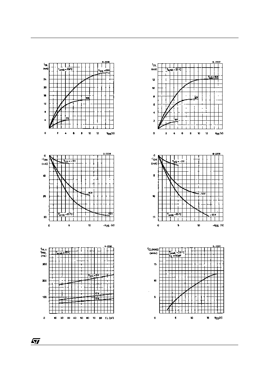
Typical Output Low (sink) Current
Characteristics.
Minimum Output Low (sink) Current
Characteristics.
Typical Output High (source) Current
Characteristics.
Minimum Output High (source) Current
Characteristics.
Typical Maximum Clock Input Frequency vs.
Supply Voltage.
Typical Propagation Delay Time vs. Load
Capacitance for Clock to Q Output.
HCF4510B/4516B
7/12

Typical Transition Time vs. Load Capacitance.
Typical Dynamic Power Dissipation vs.
Frequency.
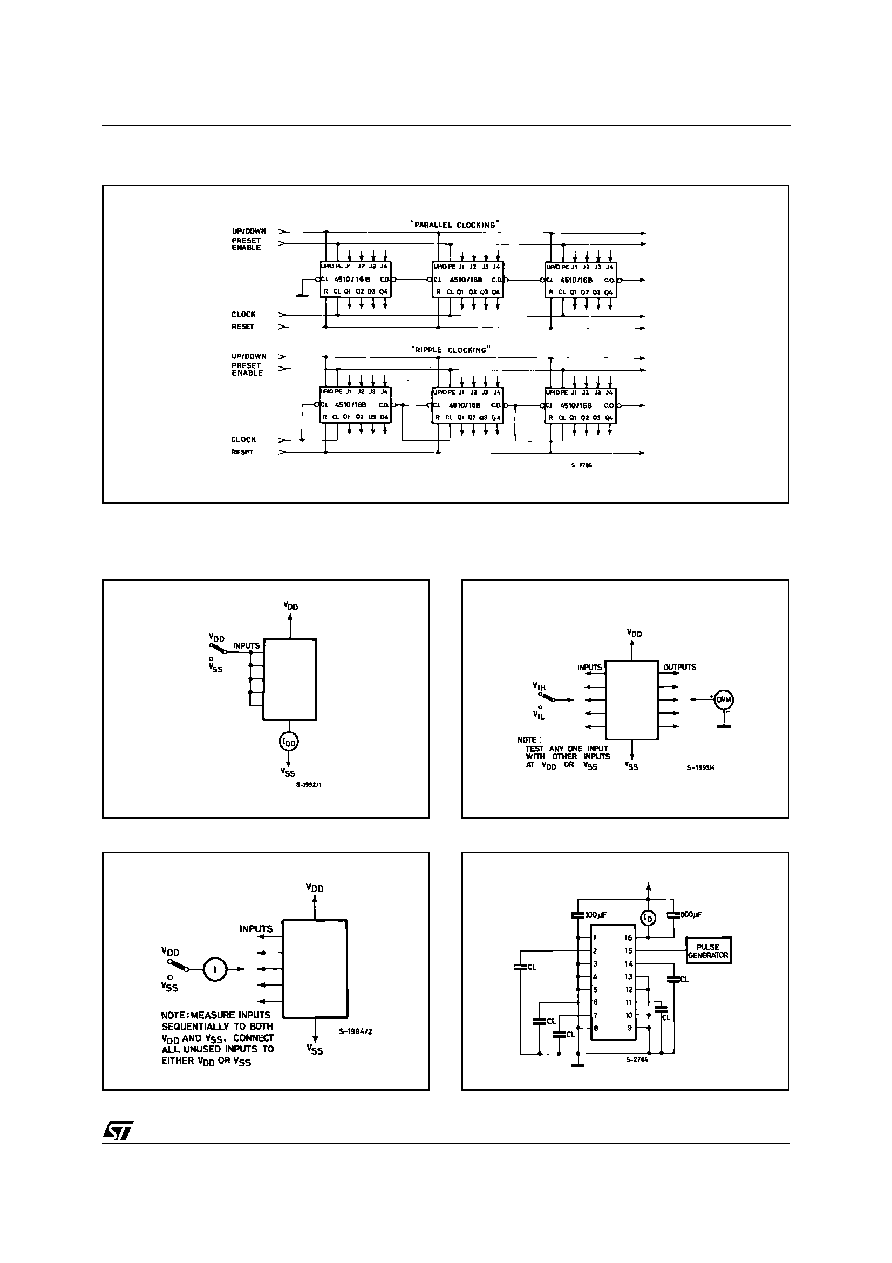
TYPICAL APPLICATIONS
Thisacquisition system can be operated in the random access mode by jamming in the channel number at the present inputs, or in the sequential mode
by clocking the HCF4516B.
TYPICAL 16-CHANNEL, 10 BIT DATA ACQUISITION SYSTEM
HCF4510B/4515B
8/12
Input Leakage Current.
Noise Immunity.
TEST CIRCUITS
Quiescent Device Current.
CASCADING COUNTER PACKAGES
Power Dissipation and Input Waveform.
HCF4510B/4516B
9/12
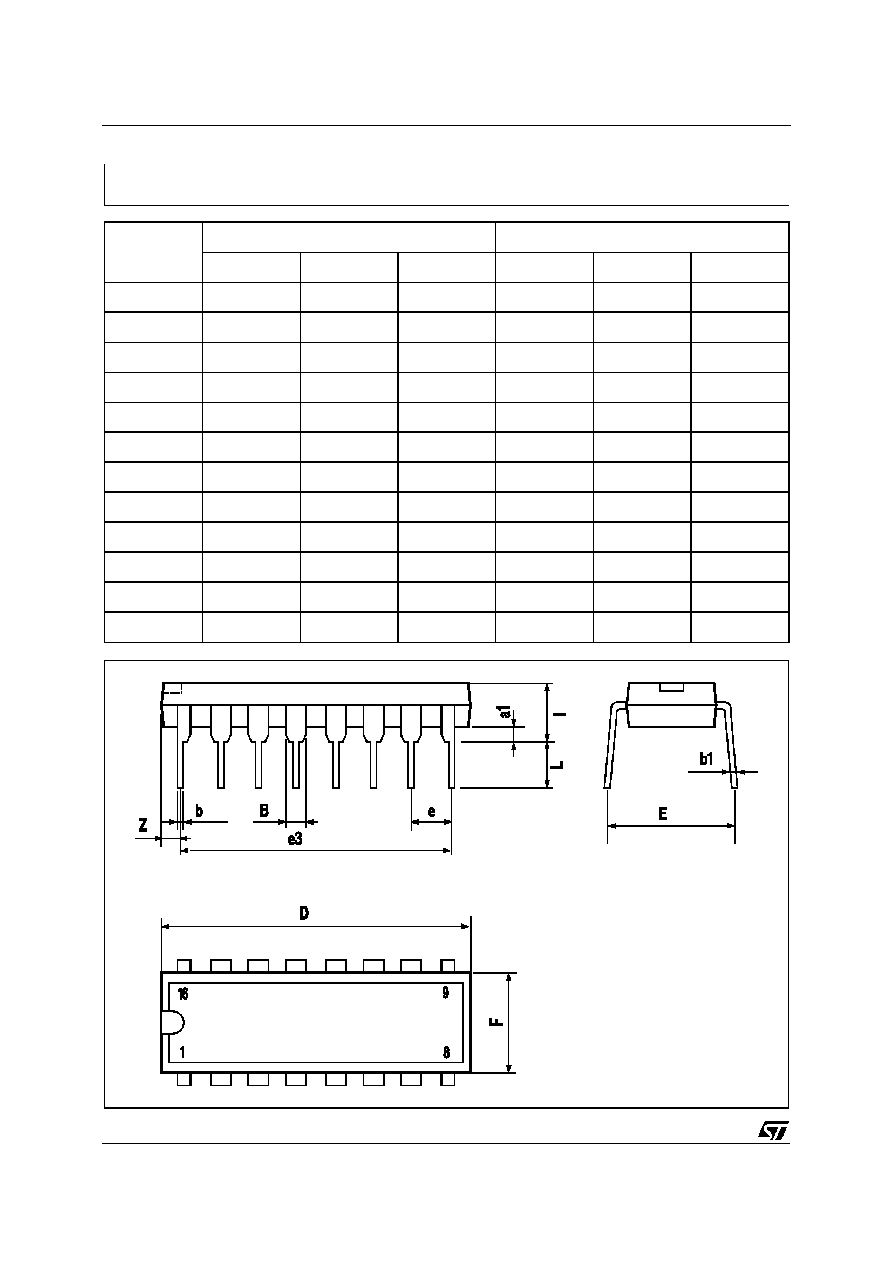
DIM.
mm
inch
MIN.
TYP.
MAX.
MIN.
TYP.
MAX.
a1
0.51
0.020
B
0.77
1.65
0.030
0.065
b
0.5
0.020
b1
0.25
0.010
D
20
0.787
E
8.5
0.335
e
2.54
0.100
e3
17.78
0.700
F
7.1
0.280
I
5.1
0.201
L
3.3
0.130
Z
1.27
0.050
P001C
Plastic DIP-16 (0.25) MECHANICAL DATA
HCF4510B/4515B
10/12
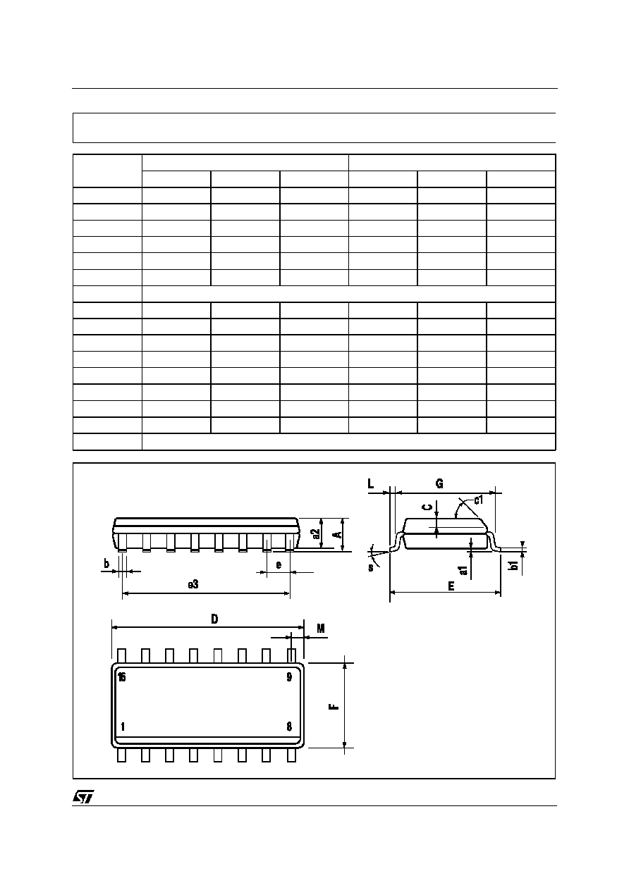
DIM.
mm
inch
MIN.
TYP.
MAX.
MIN.
TYP.
MAX.
A
1.75
0.068
a1
0.1
0.2
0.004
0.007
a2
1.65
0.064
b
0.35
0.46
0.013
0.018
b1
0.19
0.25
0.007
0.010
C
0.5
0.019
c1
45 (typ.)
D
9.8
10
0.385
0.393
E
5.8
6.2
0.228
0.244
e
1.27
0.050
e3
8.89
0.350
F
3.8
4.0
0.149
0.157
G
4.6
5.3
0.181
0.208
L
0.5
1.27
0.019
0.050
M
0.62
0.024
S
8 (max.)
P013H
SO-16 MECHANICAL DATA
HCF4510B/4516B
11/12

Information furnished is believed to be accurate and reliable. However, STMicroelectronics assumes no responsibility for the consequences
of use of such information nor for any infringement of patents or other rights of third parties which may result from its use. No license is
granted by implication or otherwise under any patent or patent rights of STMi croelectronics. Specification mentioned in this publication are
subject to change without notice. This publication supersedes and replaces all information previously supplied. STMi croelectronics products
are not authorized for use as critical components in life support devices or systems withoutexpress written approval of STMicroelectronics.
The ST logo is a registered trademark of STMicroelectronics
©
2000 STMicroelectronics ≠ Printed in Italy ≠ All Rights Reserved
STMicroelectronics GROUP OF COMPANIES
Australia - Brazil - China - Finland - France - Germany - Hong Kong - India - Italy - Japan - Malaysia - Malta - Morocco
Singapore - Spain - Sweden - Switzerland - United Kingdom - U.S.A.
http://www.st.com
.
HCF4510B/4515B
12/12