 | –≠–ª–µ–∫—Ç—Ä–æ–Ω–Ω—ã–π –∫–æ–º–ø–æ–Ω–µ–Ω—Ç: HCF4511B | –°–∫–∞—á–∞—Ç—å:  PDF PDF  ZIP ZIP |

HCC/HCF4511B
BCD-TO-SEVEN SEGMENT LATCH/DECODER/DRIVER
DESCRIPTION
.
HIGH-OUTPUT-SOURCING CAPABILITY (up
to 25 mA)
.
INPUT LATCHES FOR BCD CODE STORAGE
.
LAMP TEST AND BLANKING CAPABILITY
.
7-SEGMENT OUTPUTS BLANKED FOR BCD
INPUT CODES > 1001
.
QUIESCENT CURRENT SPECIFIED TO 20V
FOR HCC DEVICE
.
STANDARDIZED
SYMMETRICAL
OUTPUT
CHARACTERISTICS
.
5V, 10V, AND 15V PARAMETRIC RATINGS
.
INPUT CURRENT OF 100mA AT 18V AND 25
∞
C
FOR HCC DEVICE
.
100% TESTED FOR QUIESCENT CURRENT
.
MEETS ALL REQUIREMENTS OF JEDEC TEN-
TATIVE STANDARD N
∞
13A, "STANDARD SPE-
CIFICATIONS FOR DESCRIPTION OF "B"
SERIES CMOS DEVICES"
November 1996
The HCC 4511B (extended temperature range) and
the HCF 4511B (intermediate temperature range)
are monolithic integrated circuits available in 16-le-
ad dual in-line plastic or ceramic package and pla-
stic micro package.
The HCC/HCF 4511B types are BCD-to-7-segment
latch decoder drivers constructed with COS/MOS
logic and n-p-n bipolar transistor output devices on
a single monolithic structure. These devices combi-
ne the low quiescent power dissipation and high noi-
se immunity features of COS/MOS with n-p-n
bipolar output transistors capable of sourcing up to
25 mA. This capability allows the HCC/HCF 4511B
types to drive LED's and other displays directly.
Lamp Test (LT), Blanking (BL), and Latch Enable or
Strobe inputs are provided to test the display, shut
off or intensity-modulate it, and store or strobe a
BCD code, respectively. Several different signal
may be multiplexed and displayed when external
multiplexing circuitry is used.
EY
(Plastic Package)
F
(Ceramic Frit Seal Package)
C1
(Plastic Chip Carrier)
ORDER CODES :
HCC4511BF
HCF4511BM1
HCF4511BEY
HCF4511BC1
PIN CONNECTIONS
M1
(Micro Package)
1/16

FUNCTIONAL DIAGRAM
ABSOLUTE MAXIMUM RATINGS
Symbol
Parameter
Value
Unit
V
DD
*
Supply Voltage : HC C Types
H C F Types
≠ 0.5 to + 20
≠ 0.5 to + 18
V
V
V
i
Input Voltage
≠ 0.5 to V
DD
+ 0.5
V
I
I
DC Input Current (any one input)
±
10
mA
P
t o t
Total Power Dissipation (per package)
Dissipation per Output Transistor
for T
o p
= Full Package-temperature Range
200
100
mW
mW
T
o p
Operating Temperature : HCC Types
H CF Types
≠ 55 to + 125
≠ 40 to + 85
∞
C
∞
C
T
s t g
Storage Temperature
≠ 65 to + 150
∞
C
RECOMMENDED OPERATING CONDITIONS
Symbol
Parameter
Value
Unit
V
DD
Supply Voltage : H CC Types
H C F Types
3 to 18
3 to 15
V
V
V
I
Input Voltage
0 to V
DD
V
T
o p
Operating Temperature : HCC Types
H CF Types
≠ 55 to + 125
≠ 40 to + 85
∞
C
∞
C
Stresses above those listed under "Absolute Maximum Ratings" may cause permanent damage to the device. This is a stress rating only and
functionnal operation of the device at these or any other conditions above those indicated in the operational sections of this specification is not
implied. Exposure to absolute maximum rating conditions for external periods may affect device reliability.
* All voltage values are referred to V
SS
pin voltage.
HCC/HFC4511B
2/16

LOGIC DIAGRAMS
HCC/HCF4511B
3/16
TRUTH TABLE
LE
BI
L T
D C B
A
a b c d e f g
Display
X
X
0
X
X
X X
1 1 1 1 1 1 1
8
X
0
1
X X X X
0
0 0 0 0 0 0
Blank
0
1
1
0
0
0
0
1 1 1 1 1 1 0
0
0
1
1
0
0
0
1
0 1 1 0 0 0 0
1
0
1
1
0
0
1
0
1 1 0 1 1 0 1
2
0
1
1
0
0
1
1
1 1 1 1 0 0 1
3
0
1
1
0
1
0
0
0 1 1 0 0 1 1
4
0
1
1
0
1
0
1
1 0 1 1 0 1 1
5
0
1
1
0
1
1
0
0 0 1 1 1 1 1
6
0
1
1
0
1
1
1
1 1 1 0 0 0 0
7
0
1
1
1
0
0
0
1 1 1 1 1 1 1
8
0
1
1
1
0
0
1
1 1 1 0 0 1 1
9
0
1
1
1 0 1 0
0 0 0 0 0 0 0
Blank
0
1
1
1 0 1 1
0 0 0 0 0 0 0
Blank
0
1
1
1 1 0 0
0 0 0 0 0 0 0
Blank
0
1
1
1 1 0 1
0 0 0 0 0 0 0
Blank
0
1
1
1 1 1 0
0 0 0 0 0 0 0
Blank
0
1
1
1 1 1 1
0 0 0 0 0 0 0
Blank
1
1
1
X X X X
*
*
HCC/HFC4511B
4/16
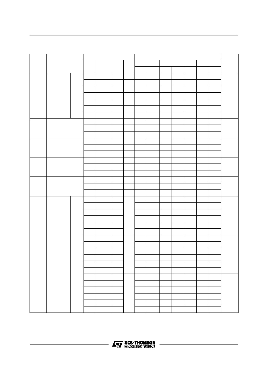
STATIC ELECTRICAL CHARACTERISTICS (over recommended operating conditions)
Test Conditions
Value
V
I
V
O
|I
O
|
V
D D
T
L o w
*
25
∞
C
T
Hi g h
*
Symbol
Parameter
(V)
(V)
(
µ
A)
(V)
Min. Max. Min. Typ. Max. Min. Max.
Unit
I
L
Quiescent
Current
HCC
Types
0/ 5
5
5
0.04
5
150
µ
A
0/10
10
10
0.04
10
300
0/15
15
20
0.04
20
600
0/20
20
100
0.08
100
3000
HCF
Types
0/ 5
5
20
0.04
20
150
0/10
10
40
0.04
40
300
0/15
15
80
0.04
80
600
V
O H
Output High
Voltage
0/ 5
5
4
4.1
4.55
4.2
V
0/10
10
9
9.1
9.55
9.2
0/15
15
14
14.1
14.55
14.2
V
O L
Output Low
Voltage
5/0
5
0.05
0.05
0.05
V
10/0
10
0.05
0.05
0.05
15/0
15
0.05
0.05
0.05
V
IH
Input High
Voltage
0.5/3.8
5
3.5
3.5
3.5
V
1/8.8
10
7
7
7
1.5/13.8
15
11
11
11
V
IL
Input Low
Voltage
3.8/0.5
5
1.5
1.5
1.5
V
8.8/1
10
3
3
3
13.8/1.5
15
4
4
4
V
O H
Output
Drive
Voltage
HCC
Types
0
5
4.1
4.10
4.55
4.20
V
5
4.25
10
3.80
3.90
4.10
3.90
15
3.95
20
3.55
3.40
3.75
25
3.40
3.10
3.55
0
10
9
9.10
9.55
9.20
V
5
9.25
10
8.85
9
9.15
15
9.05
20
8.70
8.60
8.90
8.40
25
8.60
8.30
8.75
0
15
14
14.10 14.55
14.20
V
5
14.30
10
13.90
14
14.20
14
15
14.10
20
13.75
13.70 13.95
13.50
25
13.65
13.50 13.80
13.10
* T
Low
= ≠ 55
∞
C for HCC device : ≠ 40
∞
C for HCF device.
* T
High
= + 125
∞
C for HCC device : + 85
∞
C for HCF device.
The Noise Margin for both "1" and "0" level is : 1V min. with V
DD
= 5V, 2V min. with V
DD
= 10V, 2.5 V min. with V
DD
= 15V.
HCC/HCF4511B
5/16

STATIC ELECTRICAL CHARACTERISTICS (continued)
Test Conditions
Value
V
I
V
O
|I
O
|
V
D D
T
L o w
*
25
∞
C
T
Hi g h
*
Symbol
Parameter
(V)
(V)
(
µ
A)
(V)
Min. Max. Min. Typ. Max. Min. Max.
Unit
V
O H
Output
Drive
Voltage
HCF
Types
0
5
4.1
4.1
4.57
4.1
V
5
4.24
10
3.6
3.6
4.12
3.3
15
3.94
20
2.8
2.8
3.75
2.5
25
3.54
0
10
9.1
9.1
9.58
9.1
V
5
9.26
10
8.75
8.75
9.17
8.45
15
9.04
20
8.1
8.1
8.90
7.8
25
8.75
0
15
14.1
14.1
14.59
14.1
V
5
14.27
10
13.75
13.75 14.18
13.45
15
14.07
20
13.1
13.1
13.95
12.8
25
13.80
I
O L
Output
Sink
Current
HCC
Types
0/ 5
0.4
5
0.64
0.51
1
0.36
mA
0/10
0.5
10
1.6
1.3
2.6
0.9
0/15
1.5
15
4.2
3.4
6.8
2.4
HCF
Types
0/ 5
0.4
5
0.52
0.44
1
0.36
0/10
0.5
10
1.3
1.1
2.6
0.9
0/15
1.5
15
3.6
3
6.8
2.4
I
IH
, I
IL
Input
Leakage
Current
HCC
Types
0/18
Any Input
18
±
0. 1
±
10
≠ 5
±
0.1
±
1
µ
A
HCF
Types
0/15
15
±
0.3
±
10
≠ 5
±
0.3
±
1
C
I
Input Capacitance
Any Input
5
7.5
pF
* T
Low
= ≠ 55
∞
C for HCC device : ≠ 40
∞
C for HCF device.
* T
High
= + 125
∞
C for HCC device : + 85
∞
C for HCF device.
The Noise Margin for both "1" and "0" level is : 1V min. with V
DD
= 5V, 2V min. with V
DD
= 10V, 2.5 V min. with V
DD
= 15V.
HCC/HFC4511B
6/16
DYNAMIC ELECTRICAL CHARACTERISTICS (T
amb
= 25
o
C, C
L
= 50 pF, R
L
= 200 K
,
typical temperature coefficent for all V
DD
values is 03 %/
o
C, all input rise and fall times= 20 ns)
Symbol
Parameter
Test Conditions
Value
Unit
V
DD
(V)
Min.
Typ.
Max.
t
PHL
Propagation Delay Time (data)
5
520
1040
ns
10
210
420
15
150
300
t
PLH
Propagation Delay Time (data)
5
660
1320
ns
10
260
520
15
180
360
t
PHL
Propagation Delay Time (BL)
5
350
700
ns
10
175
350
15
125
250
t
PLH
Propagation Delay Time (BL)
5
400
800
ns
10
175
350
15
150
300
t
PHL
Propagation Delay Time (LT)
5
250
500
ns
10
125
250
15
85
170
t
PLH
Propagation Delay Time (LT)
5
150
300
ns
10
75
150
15
50
100
t
TLH
Transition Time
5
40
80
ns
10
30
60
15
20
40
t
THL
Transition Time
5
125
310
ns
10
75
185
15
65
160
t
setup
Setup Time
5
150
75
ns
10
70
35
15
40
20
t
hold
Hold Time
5
0
-75
ns
10
0
-35
15
0
-20
t
W
Strobe Pulse Width
5
400
200
ms
10
160
80
15
100
50
HCC/HCF4511B
7/16
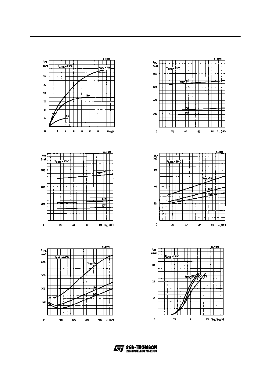
Typical Output Low (sink) Current Characteristics.
Typical data-to-output, low-to-high-level propaga-
tion delay time as a function of load capacitance.
Typical data-to-output, high-to-low-level propaga-
tion delay time as a function of load capacitance.
Typical low-to-high level transition ime as a func-
tion of load capacitance.
Typical Voltage drop (V
DD
to output) vs. Output
source Current as a Function of Supply.
Typical high-to-low level transition ime as a func-
tion of load capacitance.
HCC/HFC4511B
8/16
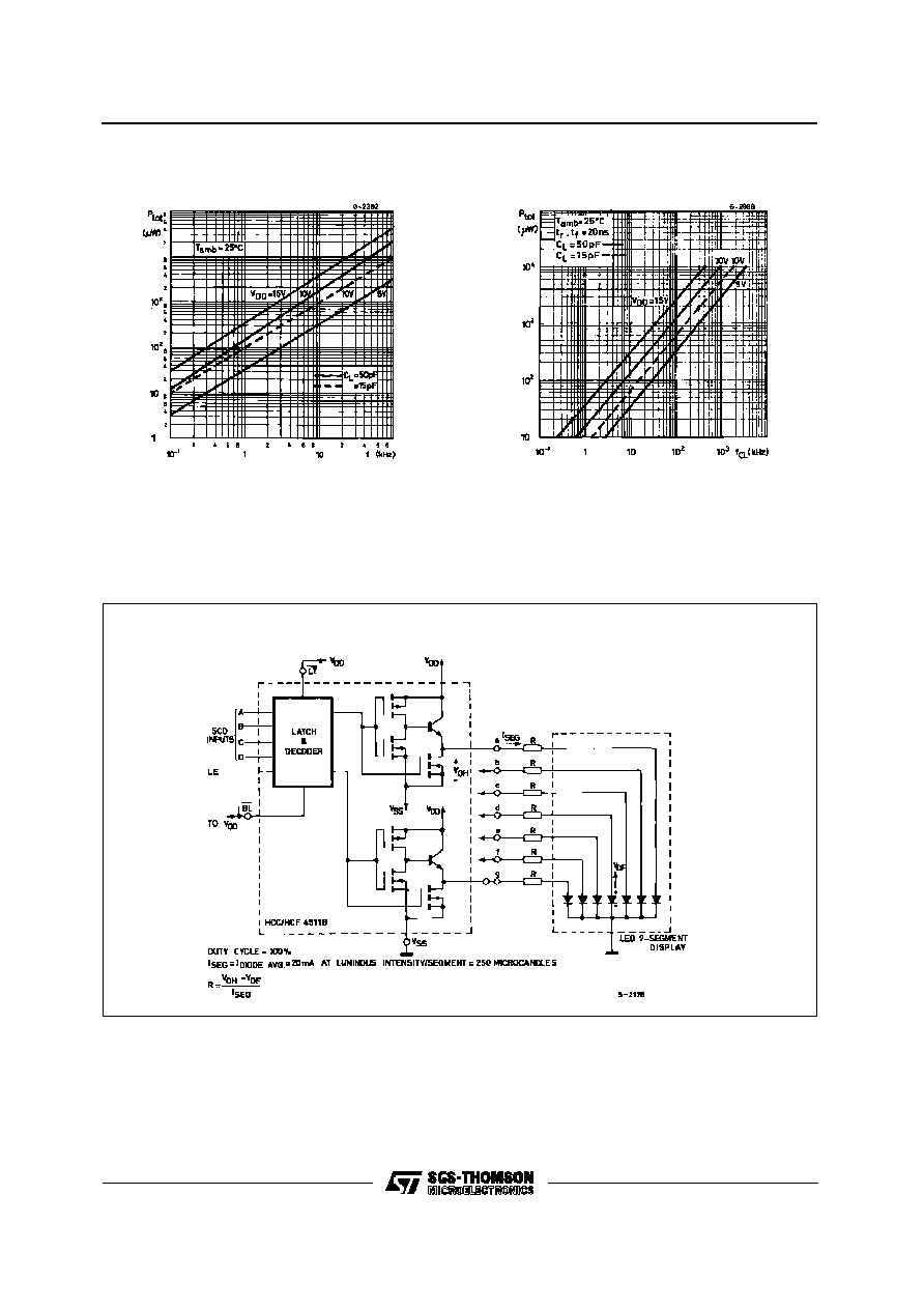
Typical Dynamic Power Dissipation Charac-
teristics.
Derated Static Output Current Per Output.
TYPICAL APPLICATIONS (interfacing with various displays)
DRIVING COMMON-CATHODE 7-SEGMENT LED DISPLAYS
Maximum continuous derated output current IOH applies to a single
output with all other outputs sourcing an equal amount of current at
the supply voltages shown. Operation above the derating curve is
not recommenced.
HCC/HCF4511B
9/16
Input Leakage Current.
Noise Immunity.
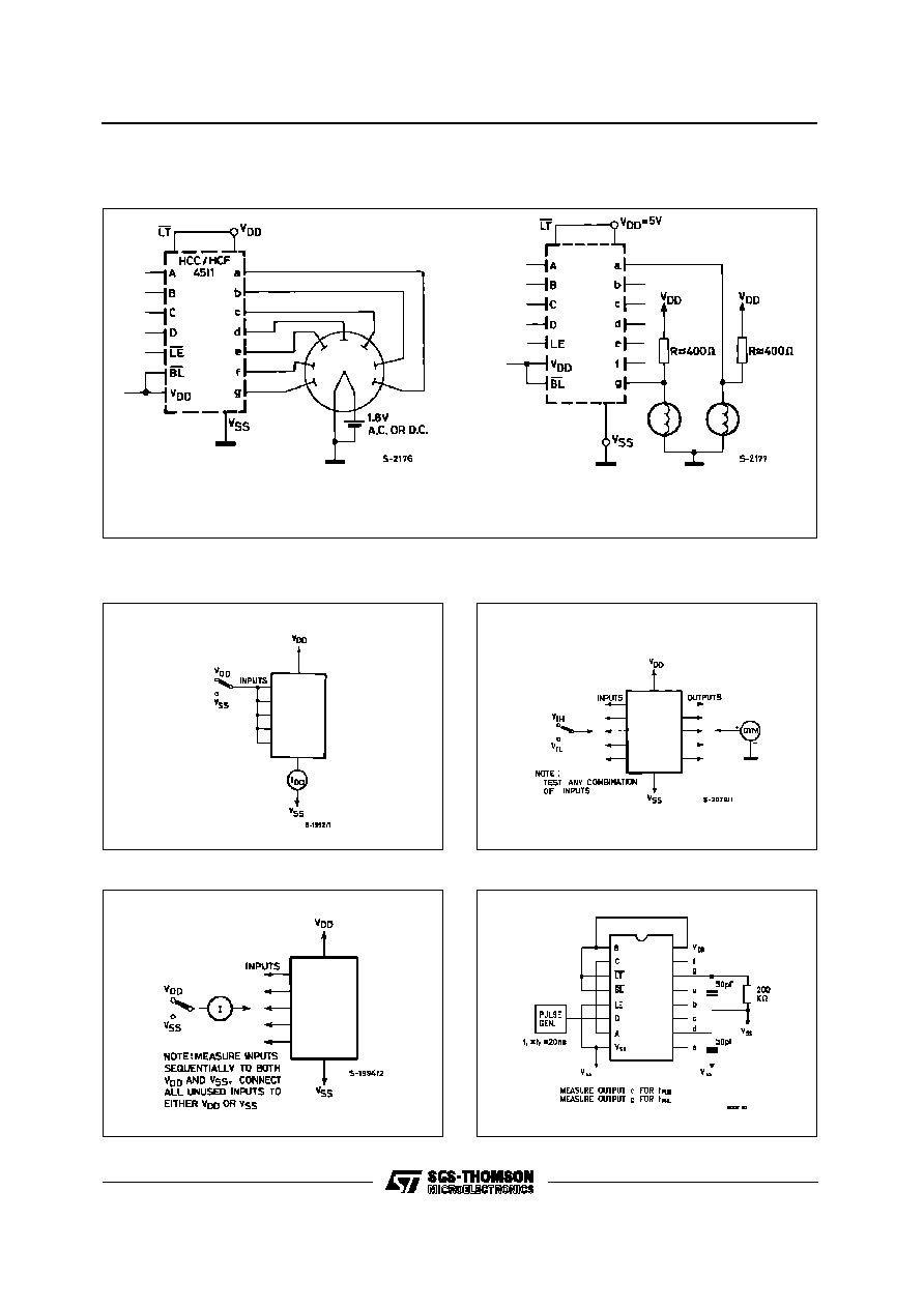
TEST CIRCUITS
Quiescent Device Current.
Driving Low-voltage Fluorescent Displays. Driving Incandescent Displays.
Data Propagation Delay.
A medium-brightness intensity display can be obtained with low-
voltage fluorescent displays such as the Tung-Sot Digivac S/G
series.
2 of 7 Segments Shown Connected
Resistors R from VDD VDD to each 7-segment driver output
are choosen to keep all Numitron segments slightly on and
warm.
TYPICAL APPLICATIONS (continued)
HCC/HFC4511B
10/16
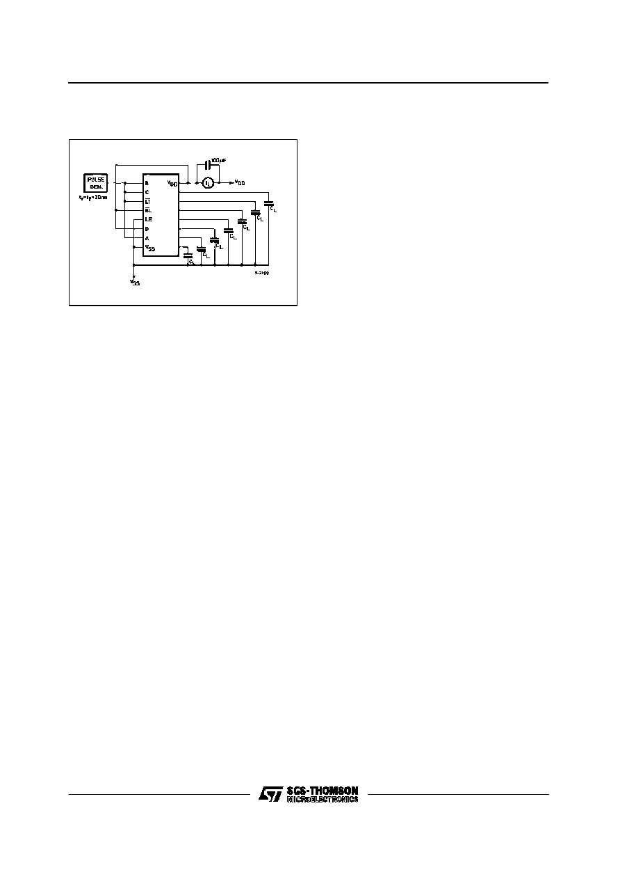
TEST CIRCUITS (continued)
Dynamic Power dissipation.
HCC/HCF4511B
11/16
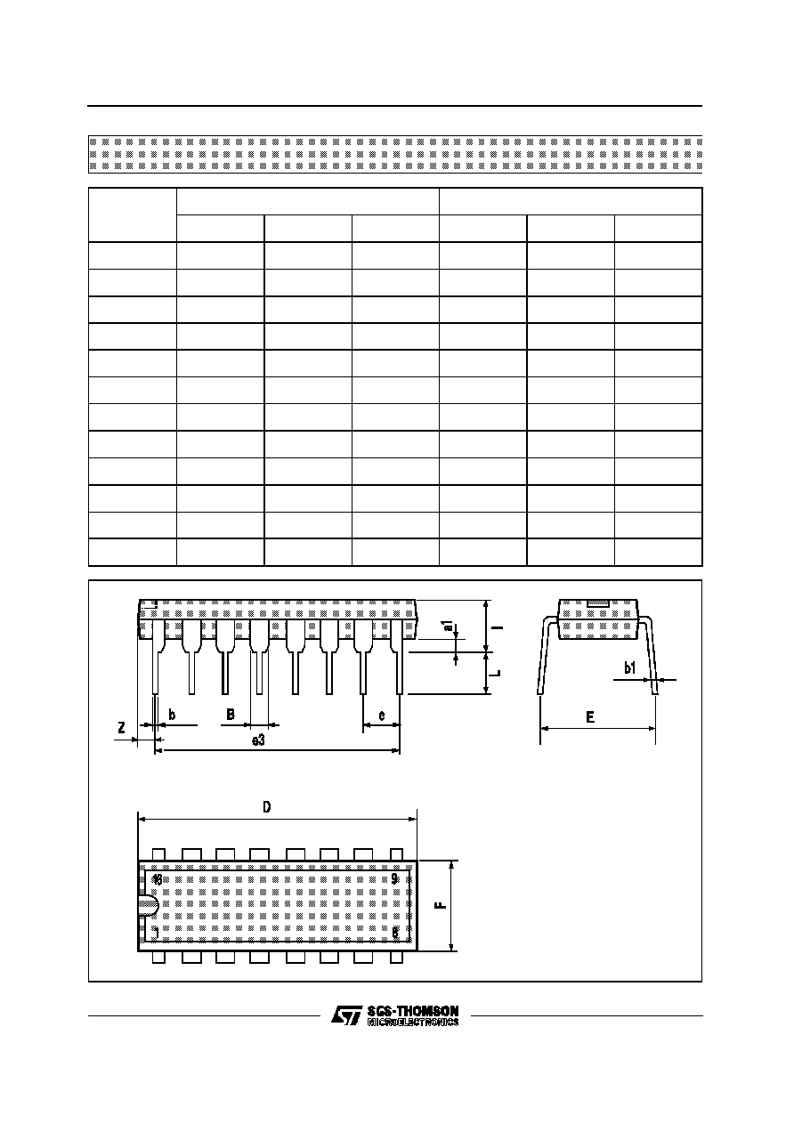
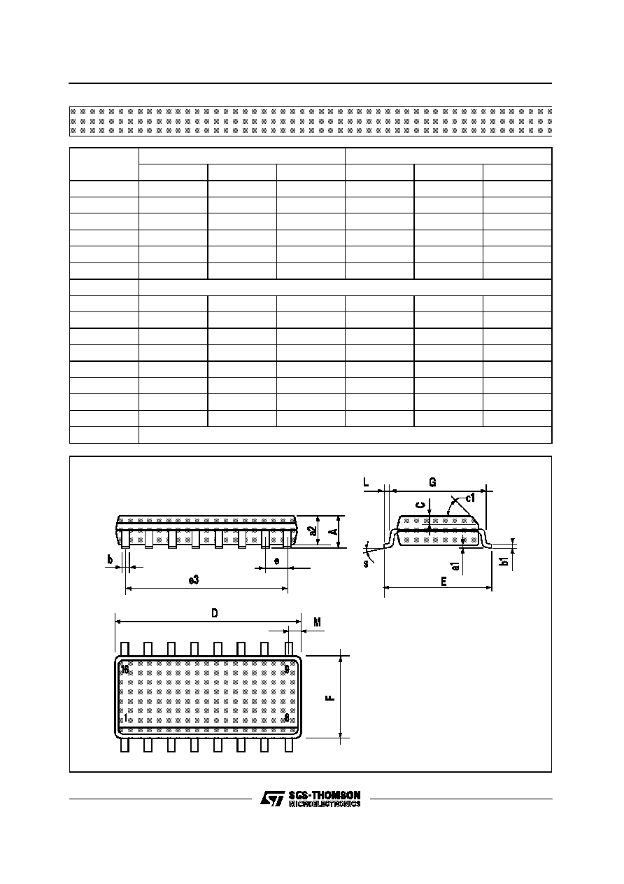
Plastic DIP16 (0.25) MECHANICAL DATA
DIM.
mm
inch
MIN.
TYP.
MAX.
MIN.
TYP.
MAX.
a1
0.51
0.020
B
0.77
1.65
0.030
0.065
b
0.5
0.020
b1
0.25
0.010
D
20
0.787
E
8.5
0.335
e
2.54
0.100
e3
17.78
0.700
F
7.1
0.280
I
5.1
0.201
L
3.3
0.130
Z
1.27
0.050
P001C
HCC/HFC4511B
12/16

Ceramic DIP16/1 MECHANICAL DATA
DIM.
mm
inch
MIN.
TYP.
MAX.
MIN.
TYP.
MAX.
A
20
0.787
B
7
0.276
D
3.3
0.130
E
0.38
0.015
e3
17.78
0.700
F
2.29
2.79
0.090
0.110
G
0.4
0.55
0.016
0.022
H
1.17
1.52
0.046
0.060
L
0.22
0.31
0.009
0.012
M
0.51
1.27
0.020
0.050
N
10.3
0.406
P
7.8
8.05
0.307
0.317
Q
5.08
0.200
P053D
HCC/HCF4511B
13/16
SO16 (Narrow) MECHANICAL DATA
DIM.
mm
inch
MIN.
TYP.
MAX.
MIN.
TYP.
MAX.
A
1.75
0.068
a1
0.1
0.2
0.004
0.007
a2
1.65
0.064
b
0.35
0.46
0.013
0.018
b1
0.19
0.25
0.007
0.010
C
0.5
0.019
c1
45
∞
(typ.)
D
9.8
10
0.385
0.393
E
5.8
6.2
0.228
0.244
e
1.27
0.050
e3
8.89
0.350
F
3.8
4.0
0.149
0.157
G
4.6
5.3
0.181
0.208
L
0.5
1.27
0.019
0.050
M
0.62
0.024
S
8
∞
(max.)
P013H
HCC/HFC4511B
14/16
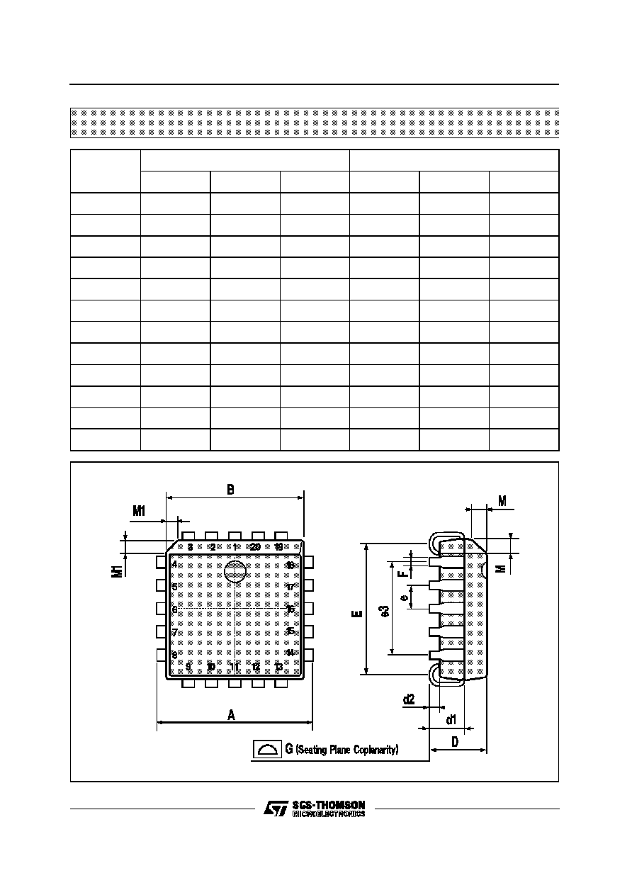
PLCC20 MECHANICAL DATA
DIM.
mm
inch
MIN.
TYP.
MAX.
MIN.
TYP.
MAX.
A
9.78
10.03
0.385
0.395
B
8.89
9.04
0.350
0.356
D
4.2
4.57
0.165
0.180
d1
2.54
0.100
d2
0.56
0.022
E
7.37
8.38
0.290
0.330
e
1.27
0.050
e3
5.08
0.200
F
0.38
0.015
G
0.101
0.004
M
1.27
0.050
M1
1.14
0.045
P027A
HCC/HCF4511B
15/16

Information furnished is believed to be accurate and reliable. However, SGS-THOMSON Microelectronics assumes no responsability for the
consequences of use of such information nor for any infringement of patents or other rights of third parties which may results from its use. No
license is granted by implication or otherwise under any patent or patent rights of SGS-THOMSON Microelectronics. Specifications mentioned
in this publication are subject to change without notice. This publication supersedes and replaces all information previously supplied.
SGS-THOMSON Microelectronics products are not authorized for use as critical components in life support devices or systems without express
written approval of SGS-THOMSON Microelectonics.
©
1996 SGS-THOMSON Microelectronics - Printed in Italy - All Rights Reserved
SGS-THOMSON Microelectronics GROUP OF COMPANIES
Australia - Brazil - Canada - China - France - Germany - Hong Kong - Italy - Japan - Korea - Malaysia - Malta - Morocco - The Netherlands -
Singapore - Spain - Sweden - Switzerland - Taiwan - Thailand - United Kingdom - U.S.A
.
HCC/HFC4511B
16/16