 | –≠–ª–µ–∫—Ç—Ä–æ–Ω–Ω—ã–π –∫–æ–º–ø–æ–Ω–µ–Ω—Ç: HCF4514B | –°–∫–∞—á–∞—Ç—å:  PDF PDF  ZIP ZIP |
HCC/HCF4514B
HCC/HCF4515B
4-BIT LATCH/4-TO-16 LINE DECODER
DESCRIPTION
June 1989
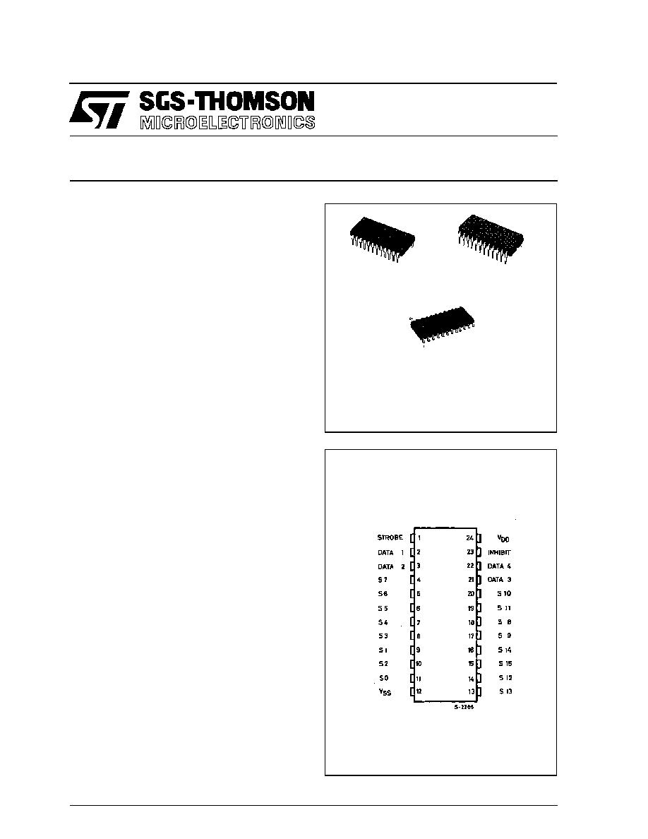
EY
(Plastic Package)
F
(Ceramic Frit Seal Package)
M1
(Micro Package)
ORDER CODES :
HCC45XXBF
HCF45XXBEY
HCF45XXBM1
PIN CONNECTIONS
HCC/HCF4514B OUTPUT "HIGH" ON SELECT
HCC/HCF4515B OUTPUT "LOW" ON SELECT
.
QUIESCENT CURRENT SPECIFIED TO 20V
FOR HCC DEVICE
.
STROBED INPUT LATCH
.
INHIBIT CONTROL
.
INPUT CURRENT OF 100nA AT 18V AND 25
∞
C
FOR HCC DEVICE
.
100% TESTED FOR QUIESCENT CURRENT
.
MEETS ALL REQUIREMENTS OF JEDEC TEN-
TATIVE STANDARD N
0
. 13A, "STANDARD
SPECIFICATIONS FOR DESCRIPTION OF "B"
SERIES CMOS DEVICES"
The HCC 4514B/HCC4515B (extended temperature
range) and the HCF 4514B/HCF4515B (intermediate
temperature range) are monolithic integrated circuits
available in 24-lead dual in-line plastic or ceramic
package
and
plastic
micro
package.
The
HCC/HCF4514B/4515B consisting of a 4-bit strobed
latch and a 4 to 16 line decoder. The latches hold the
last input data presented prior to the strobe transition
from 1 to 0. Inhibit control allows all outputs to be
placed at 0 (HCC/HCF4514B) or 1 (HCC/HCF4515B)
regardless of the state ofthe data or strobe inputs. The
decode truth table indicates all combinations of data
inputs and appropriate selected outputs.
1/11

FUNCTIONAL DIAGRAM
ABSOLUTE MAXIMUM RATINGS
Symbol
Parameter
Value
Unit
V
DD
*
Supply Voltage : HC C Types
H C F Types
≠ 0.5 to + 20
≠ 0.5 to + 18
V
V
V
i
Input Voltage
≠ 0.5 to V
DD
+ 0.5
V
I
I
DC Input Current (any one input)
±
10
mA
P
t o t
Total Power Dissipation (per package)
Dissipation per Output Transistor
for T
o p
= Full Package-temperature Range
200
100
mW
mW
T
o p
Operating Temperature : HCC Types
H CF Types
≠ 55 to + 125
≠ 40 to + 85
∞
C
∞
C
T
s t g
Storage Temperature
≠ 65 to + 150
∞
C
RECOMMENDED OPERATING CONDITIONS
Symbol
Parameter
Value
Unit
V
DD
Supply Voltage : H CC Types
H C F Types
3 to 18
3 to 15
V
V
V
I
Input Voltage
0 to V
DD
V
T
o p
Operating Temperature : HCC Types
H CF Types
≠ 55 to + 125
≠ 40 to + 85
∞
C
∞
C
Stresses above those listed under "Absolute Maximum Ratings" may cause permanent damage to the device. This is a stress
rating only and functional operation of the device at these or any other conditions above those indicated in the operational sec-
tions of this specifi cation is not implied. Exposure to absolute maximum rating conditions for external periods may affect device
reliability.
HCC/HCF4514B/4515B
2/11

LOGIC DIAGRAM AND TRUTH TABLE
D a t a
Inputs
Inhibit
D C B A
Se lec ted Output
H C C /H C F 4 5 1 4 B = Logic 1
(H igh)
H C C /H C F 4 5 1 5 B = Logic 0
(Low)
0
0
0
0
0
0
0
0
0
0
0
0
0
0
1
1
0
1
0
1
S0
S1
S2
S3
0
0
0
0
0
0
0
0
1
1
1
1
0
0
1
1
0
1
0
1
S4
S5
S6
S7
0
0
0
0
1
1
1
1
0
0
0
0
0
0
1
1
0
1
0
1
S8
S9
S10
S11
0
0
0
0
1
1
1
1
1
1
1
1
0
0
1
1
0
1
0
1
S12
S13
S14
S15
1
X X X X All Outputs = 0, HCC/HCF 4514 B
All Outputs = 1, HCC/HCF 4515 B
WAVEFORMS
X = Don't Care
1 = high
Setup Time and Strobe Pulse Width.
Strobe = 1
HCC/HCF4514B/4515B
3/11

STATIC ELECTRICAL CHARACTERISTICS (over recommended operating conditions)
Test Conditions
Value
V
I
V
O
|I
O
|
V
D D
T
L o w
*
25
∞
C
T
Hi g h
*
Symbol
Parameter
(V)
(V)
(
µ
A)
(V)
Min. Max. Min. Typ. Max. Min. Max.
Unit
I
L
Quiescent
Current
HCC
Types
0/ 5
5
5
0.04
5
150
µ
A
0/10
10
10
0.04
10
300
0/15
15
20
0.04
20
600
0/20
20
100
0.08
100
3000
HCF
Types
0/ 5
5
20
0.04
20
150
0/10
10
40
0.04
40
300
0/15
15
80
0.04
80
600
V
O H
Output High
Voltage
0/ 5
< 1
5
4.95
4.95
4.95
V
0/10
< 1
10
9.95
9.95
9.95
0/15
< 1
15
14.95
14.95
14.95
V
O L
Output Low
Voltage
5/0
< 1
5
0.05
0.05
0.05
V
10/0
< 1
10
0.05
0.05
0.05
15/0
< 1
15
0.05
0.05
0.05
V
IH
Input High
Voltage
0.5/4.5
< 1
5
3.5
3.5
3.5
V
1/9
< 1
10
7
7
7
1.5/13.5
< 1
15
11
11
11
V
IL
Input Low
Voltage
4.5/0.5
< 1
5
1.5
1.5
1.5
V
9/1
< 1
10
3
3
3
13.5/1.5
< 1
15
4
4
4
I
O H
Output
Drive
Current
HCC
Types
0/ 5
2.5
5
≠ 2
≠ 1.6 ≠ 3.2
≠ 1.15
mA
0/ 5
4.6
5
≠ 0.64
≠ 0.51 ≠ 1
≠ 0.36
0/10
9.5
10
≠ 1.6
≠ 1.3 ≠ 2.6
≠ 0.9
0/15
13.5
15
≠ 4.2
≠ 3.4 ≠ 6.8
≠ 2.4
HCF
Types
0/ 5
2.5
5
≠ 1.53
≠ 1.36 ≠ 3.2
≠ 1.1
0/ 5
4.6
5
≠ 0.52
≠ 0.44 ≠ 1
≠ 0.36
0/10
9.5
10
≠ 1.3
≠ 1.1 ≠ 2.6
≠ 0.9
0/15
13.5
15
≠ 3.6
≠ 3.0 ≠ 6.8
≠ 2.4
I
O L
Output
Sink
Current
HCC
Types
0/ 5
0.4
5
0.64
0.51
1
0.36
mA
0/10
0.5
10
1.6
1.3
2.6
0.9
0/15
1.5
15
4.2
3.4
6.8
2.4
HCF
Types
0/ 5
0.4
5
0.52
0.44
1
0.36
0/10
0.5
10
1.3
1.1
2.6
0.9
0/15
1.5
15
3.6
3.0
6.8
2.4
I
IH
, I
IL
Input
Leakage
Current
HCC
Types
0/18
Any Input
18
±
0.1
±
10
≠ 5
±
0.1
±
1
µ
A
HCF
Types
0/15
15
±
0.3
±
10
≠ 5
±
0.3
±
1
C
I
Input Capacitance
Any Input
5
7.5
pF
* T
Lo w
= ≠ 55
∞
C for HCC device : ≠ 40
∞
C for HCF device.
* T
High
= + 125
∞
C for HCC device : + 85
∞
C for HCF device.
The Noise Margin for both "1" and "0" level is : 1V min. with V
DD
= 5V, 2V min. with V
DD
= 10V, 2.5 V min. with V
DD
= 15V.
HCC/HCF4514B/4515B
4/11
DYNAMIC ELECTRICAL CHARACTERISTICS
(T
am b
= 25
∞
C, C
L
= 50pF, R
L
= 200k
, all input rise and fall time = 20ns)
Test Conditions
Val ue
Symbol
Parameter
V
D D
(V)
Min.
Typ.
Max.
Unit
t
PHL
,
t
P L H
Propagation Delay Time
Strobe or Data
5
485
970
ns
10
185
370
15
135
270
Inhibit
5
250
500
ns
10
110
220
15
85
170
t
T HL
,
t
T HL
Transition Time
5
100
200
ns
10
50
100
15
40
80
t
W
Strobe Pulse Width
5
250
125
ns
10
100
50
15
75
40
t
se t u p
Setup Time
5
150
75
ns
10
70
35
15
40
20
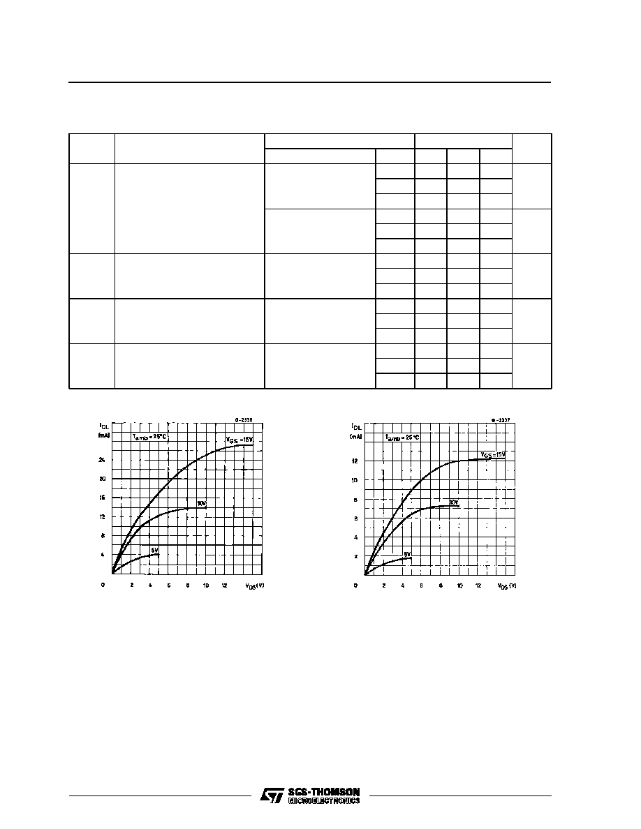
Typical Output Low (sink) Current Characteristics.
Minimum Output Low (sink) Current Characteristics.
HCC/HCF4514B/4515B
5/11

Typical Output High (source) Current Charac-
teristics.
Minimum Output High (source) Current Charac-
teristics.
Typical Strobe or Data Propagation Delay Time vs.
Load Capacitance.
Typical Inhibit Propagation Delay Time vs. Load Ca-
pacitance.
Typical Strobe or Data Propagation Delay Time vs.
Supply Voltage.
Typical Transition Time vs. Load Capacitance.
HCC/HCF4514B/4515B
6/11

Typical Power Dissipation vs. Frequency.
Noise Immunity.
TEST CIRCUITS
Quiescent Device Current.
Input Leakage Current.
HCC/HCF4514B/4515B
7/11

Plastic DIP24 (0.25) MECHANICAL DATA
DIM.
mm
inch
MIN.
TYP.
MAX.
MIN.
TYP.
MAX.
a1
0.63
0.025
b
0.45
0.018
b1
0.23
0.31
0.009
0.012
b2
1.27
0.050
D
32.2
1.268
E
15.2
16.68
0.598
0.657
e
2.54
0.100
e3
27.94
1.100
F
14.1
0.555
I
4.445
0.175
L
3.3
0.130
P043A
HCC/HCF4514B/4515B
8/11

Ceramic DIP24 MECHANICAL DATA
DIM.
mm
inch
MIN.
TYP.
MAX.
MIN.
TYP.
MAX.
A
32.3
1.272
B
13.05
13.36
0.514
0.526
C
3.9
5.08
0.154
0.200
D
3
0.118
E
0.5
1.78
0.020
0.070
e3
27.94
1.100
F
2.29
2.79
0.090
0.110
G
0.4
0.55
0.016
0.022
I
1.17
1.52
0.046
0.060
L
0.22
0.31
0.009
0.012
M
1.52
2.49
0.060
0.098
N1
4
∞
(min.), 15
∞
(max.)
P
15.4
15.8
0.606
0.622
Q
5.71
0.225
P058C
HCC/HCF4514B/4515B
9/11

SO24 MECHANICAL DATA
DIM.
mm
inch
MIN.
TYP.
MAX.
MIN.
TYP.
MAX.
A
2.65
0.104
a1
0.10
0.20
0.004
0.007
a2
2.45
0.096
b
0.35
0.49
0.013
0.019
b1
0.23
0.32
0.009
0.012
C
0.50
0.020
c1
45
∞
(typ.)
D
15.20
15.60
0.598
0.614
E
10.00
10.65
0.393
0.420
e
1.27
0.05
e3
13.97
0.55
F
7.40
7.60
0.291
0.299
L
0.50
1.27
0.19
0.050
S
8
∞
(max.)
F
C
L
E
a1
b1
A
e
D
e3
b
24
13
1
12
c1
s
a2
HCC/HCF4514B/4515B
10/11

Information furnished is believed to be accurate and reliable. However, SGS-THOMSON Microelectronics assumes no responsability for the
consequences of use of such information nor for any infringement of patents or other rights of third parties which may results from its use. No
license is granted by implication or otherwise under any patent or patent rights of SGS-THOMSON Microelectronics. Specifications mentioned
in this publication are subject to change without notice. This publication supersedes and replaces all information previously supplied.
SGS-THOMSON Microelectronics products are not authorized for use as critical components in life support devices or systems without express
written approval of SGS-THOMSON Microelectonics.
©
1994 SGS-THOMSON Microelectronics - All Rights Reserved
SGS-THOMSON Microelectronics GROUP OF COMPANIES
Australia - Brazil - France - Germany - Hong Kong - Italy - Japan - Korea - Malaysia - Malta - Morocco - The Netherlands -
Singapore - Spain - Sweden - Switzerland - Taiwan - Thailand - United Kingdom - U.S.A
HCC/HCF4514B/4515B
11/11