1/11
September 2002
s
MEDIUM SPEED OPERATION :
8 MHz (Typ.) at 10V
s
SYNCHRONOUS INTERNAL CARRY
PROPAGATION
s
RESET AND PRESET CAPABILITY
s
STANDARDIZED SYMMETRICAL OUTPUT
CHARACTERISTICS
s
QUIESCENT CURRENT SPECIF. UP TO 20V
s
5V, 10V AND 15V PARAMETRIC RATINGS
s
INPUT LEAKAGE CURRENT
I
I
= 100nA (MAX) AT V
DD
= 18V T
A
= 25įC
s
100% TESTED FOR QUIESCENT CURRENT
s
MEETS ALL REQUIREMENTS OF JEDEC
JESD13B "STANDARD SPECIFICATIONS
FOR DESCRIPTION OF B SERIES CMOS
DEVICES"
DESCRIPTION
HCF4516B is a monolithic integrated circuit
fabricated in Metal Oxide Semiconductor
technology available in DIP package.
It is a PRESETTABLE BINARY UP/DOWN
COUNTER, consists of four synchronously
clocked D-type flip-flops (with a gating structure to
provide T-type flip-flop capability) connected as a
counter. This counter can be cleared by a high
level on the RESET line, and can be preset to any
binary number present on the jam inputs by a high
level on the PRESET ENABLE line. Synchronous
cascading is accomplished by connecting all clock
inputs in parallel and connecting the CARRY OUT
of a less significant stage to the CARRY IN of a
more significant stage. HCF4516B can be
cascaded in the ripple mode by connecting all
clock inputs in parallel and connecting the CARRY
OUT to the clock of the next stage. If the UP/
DOWN input changes during a terminal count, the
CARRY OUT must be gated with the clock, and
the UP/DOWN input must change while the clock
is high. This method provides a clean clock signal
to the subsequent counting stage.
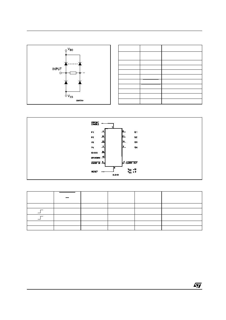
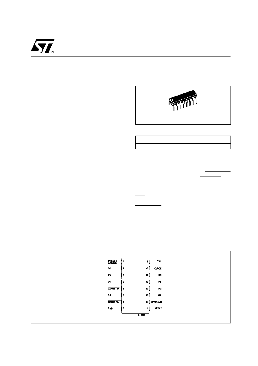
HCF4516B
PRESETTABLE BINARY UP/DOWN COUNTER
PIN CONNECTION
ORDER CODES
PACKAGE
TUBE
T & R
DIP
HCF4516BEY
DIP

HCF4516B
4/11
ABSOLUTE MAXIMUM RATINGS
Absolute Maximum Ratings are those values beyond which damage to the device may occur. Functional operation under these conditions is
not implied.
All voltage values are referred to V
SS
pin voltage.
RECOMMENDED OPERATING CONDITIONS
Symbol
Parameter
Value
Unit
V
DD
Supply Voltage
-0.5 to +22
V
V
I
DC Input Voltage
-0.5 to V
DD
+ 0.5
V
I
I
DC Input Current
Ī
10
mA
P
D
Power Dissipation per Package
200
mW
Power Dissipation per Output Transistor
100
mW
T
op
Operating Temperature
-55 to +125
įC
T
stg
Storage Temperature
-65 to +150
įC
Symbol
Parameter
Value
Unit
V
DD
Supply Voltage
3 to 20
V
V
I
Input Voltage
0 to V
DD
V
T
op
Operating Temperature
-55 to 125
įC