DUAL 64-STAGE STATIC SHIFT REGISTER
1/8
September 2002
s
CLOCK FREQUENCY 12MHz (Typ.)
at V
DD
= 10V
s
SCHMITT TRIGGER CLOCK INPUTS
ALLOWS OPERATION WITH VERY SLOW
CLOCK RISE AND FALL TIMES
s
THREE STATE OUTPUTS
s
QUIESCENT CURRENT SPECIFIED UP TO
20V
s
STANDARDIZED, SYMMETRICAL OUTPUT
CHARACTERISTCS
s
5V, 10V AND 15V PARAMETRIC RATINGS
s
INPUT LEAKAGE CURRENT
I
I
= 100nA (MAX) AT V
DD
= 18V T
A
= 25°C
s
100% TESTED FOR QUIESCENT CURRENT
s
MEETS ALL REQUIREMENTS OF JEDEC
JESD13B "STANDARD SPECIFICATIONS
FOR DESCRIPTION OF B SERIES CMOS
DEVICES"
DESCRIPTION
HCF4517B is a monolithic integrated circuit
fabricated in Metal Oxide Semiconductor
technology available in DIP package.
This device is a dual 64-stage static shift register
consisting of two independent registers each
having a clock, data, and write enable input and
outputs accessible by stages following the 16th,
32nd, 48th, and 64th stages. These stages also
serve as input points allowing data to be put in at
the 17th , 33rd, and 49th stages when the write
enable input is a logic 1 and the clock goes
through a low to high transition. The truth table
indicates how the clock and write enable inputs
control the operation of HCF4517B. Inputs at the
intermediate stages allow entry of 64-bits into the
register with 16 clock pulses. The 3-state outputs
permit connection of this device to an external
bus.
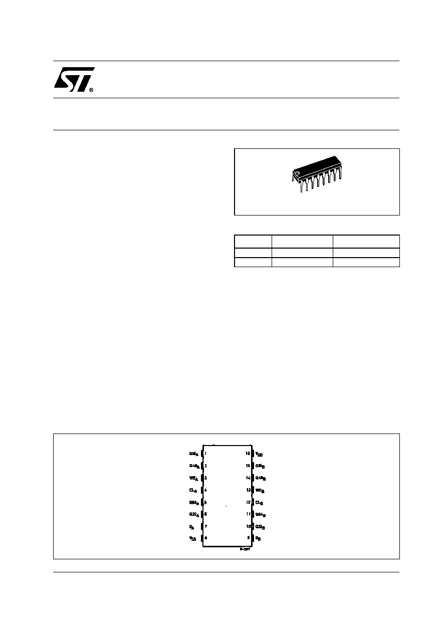
HCF4517B
DUAL 64 STAGE STATIC SHIFT REGISTER
PIN CONNECTION
ORDER CODES
PACKAGE
TUBE
T & R
DIP
HCF4517BEY
SOP
HCF4517BM1
HCF4517M013TR
DIP
HCF4517B
2/8
INPUT EQUIVALENT CIRCUIT
PIN DESCRIPTION
FUNCTIONAL DIAGRAM (One Half)
TRUTH TABLES
X : Don't Care
PIN No
SYMBOL
NAME AND FUNCTION
1, 2, 5, 6
QnA
IN/OUT Stage
10, 11,14, 15
QnB
IN/OUT Stage
3, 13
WEA, WEB
Write Enable
7, 9
DA, DB
Data Input
4, 12
CLA, CLB
Clock
8
V
SS
Negative Supply Voltage
16
V
DD
Positive Supply Voltage
CLOCK
WRITE
ENABLE
DATA
STAGE 16 TAP STAGE 32 TAP STAGE 48 TAP STAGE 64 TAP
L
L
X
Q16
Q32
Q48
Q64
L
H
X
Z
Z
Z
Z
H
L
X
Q16
Q32
Q48
Q64
H
H
X
Z
Z
Z
Z
L
DI In
Q16
Q32
Q48
Q64
H
DI In
D17 In
D33 In
D49 In
Z
L
X
Q16
Q32
Q48
Q64
H
X
Z
Z
Z
Z
HCF4517B
3/8
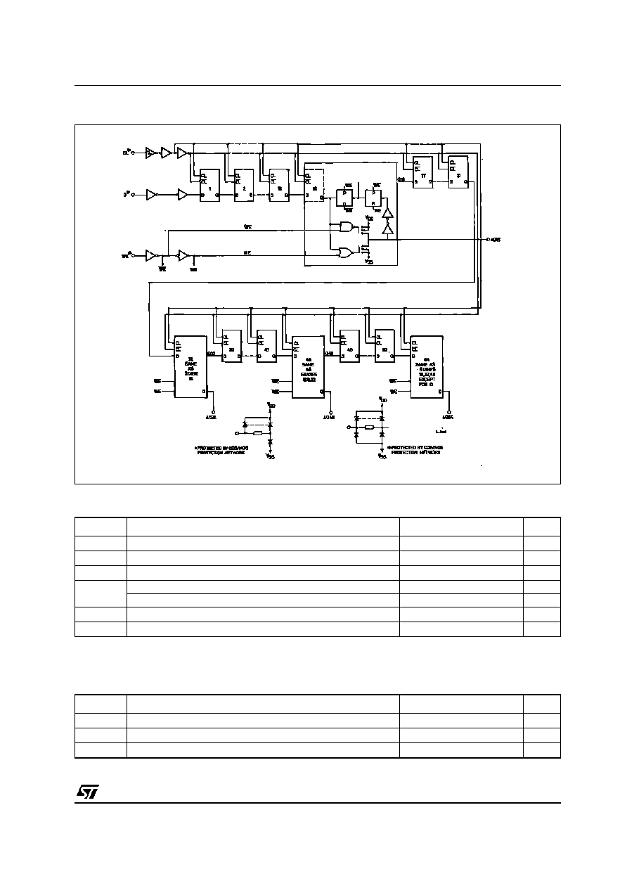
LOGIC DIAGRAM
ABSOLUTE MAXIMUM RATINGS
Absolute Maximum Ratings are those values beyond which damage to the device may occur. Functional operation under these conditions is
not implied.
All voltage values are referred to V
SS
pin voltage.
RECOMMENDED OPERATING CONDITIONS
Symbol
Parameter
Value
Unit
V
DD
Supply Voltage
-0.5 to +22
V
V
I
DC Input Voltage
-0.5 to V
DD
+ 0.5
V
I
I
DC Input Current
±
10
mA
P
D
Power Dissipation per Package
200
mW
Power Dissipation per Output Transistor
100
mW
T
op
Operating Temperature
-55 to +125
°C
T
stg
Storage Temperature
-65 to +150
°C
Symbol
Parameter
Value
Unit
V
DD
Supply Voltage
3 to 20
V
V
I
Input Voltage
0 to V
DD
V
T
op
Operating Temperature
-55 to 125
°C
HCF4517B
4/8
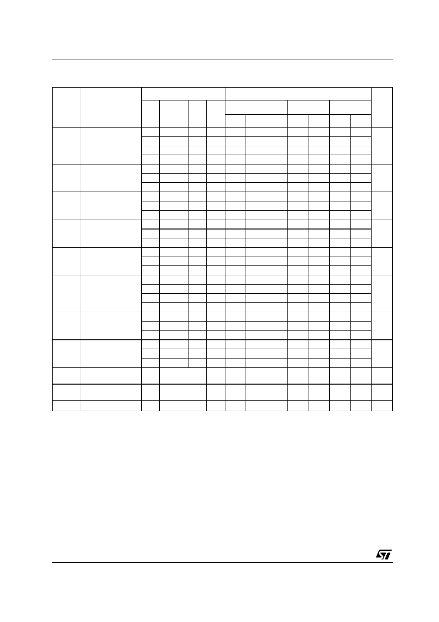
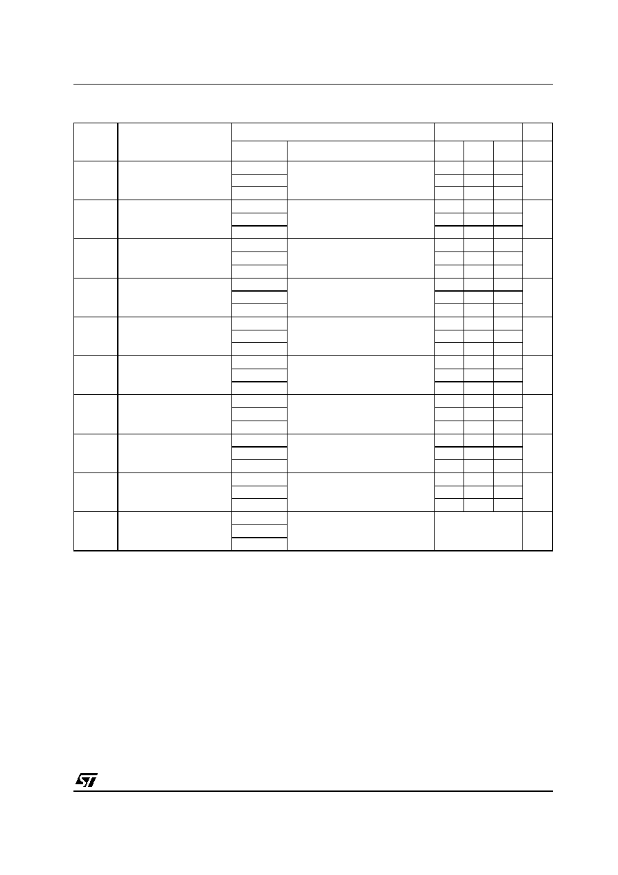
DC SPECIFICATIONS
The Noise Margin for both "1" and "0" level is: 1V min. with V
DD
=5V, 2V min. with V
DD
=10V, 2.5V min. with V
DD
=15V
Symbol
Parameter
Test Condition
Value
Unit
V
I
(V)
V
O
(V)
|I
O
|
(
µ
A)
V
DD
(V)
T
A
= 25°C
-40 to 85°C
-55 to 125°C
Min.
Typ.
Max.
Min.
Max.
Min.
Max.
I
L
Quiescent Current
0/5
5
0.04
5
150
150
µ
A
0/10
10
0.04
10
300
300
0/15
15
0.04
20
600
600
0/20
20
0.08
100
3000
3000
V
OH
High Level Output
Voltage
0/5
<1
5
4.95
4.95
4.95
V
0/10
<1
10
9.95
9.95
9.95
0/15
<1
15
14.95
14.95
14.95
V
OL
Low Level Output
Voltage
5/0
<1
5
0.05
0.05
0.05
V
10/0
<1
10
0.05
0.05
0.05
15/0
<1
15
0.05
0.05
0.05
V
IH
High Level Input
Voltage
0.5/4.5
<1
5
3.5
3.5
3.5
V
1/9
<1
10
7
7
7
1.5/13.5
<1
15
11
11
11
V
IL
Low Level Input
Voltage
4.5/0.5
<1
5
1.5
1.5
1.5
V
9/1
<1
10
3
3
3
13.5/1.5
<1
15
4
4
4
I
OH
Output Drive
Current
0/5
2.5
<1
5
-1.36
-3.2
-1.1
-1.1
mA
0/5
4.6
<1
5
-0.44
-1
-0.36
-0.36
0/10
9.5
<1
10
-1.1
-2.6
-0.9
-0.9
0/15
13.5
<1
15
-3.0
-6.8
-2.4
-2.4
I
OL
Output Sink
Current Q
0/5
0.4
<1
5
1.74
4
1.43
1.43
mA
0/10
0.5
<1
10
4.42
10.4
3.74
3.74
0/15
1.5
<1
15
11.56
27.2
9.52
9.52
I
OL
Output Sink
Current
0/5
0.4
<1
5
0.44
1
0.36
0.36
mA
0/10
0.5
<1
10
1.1
2.6
0.9
0.9
0/15
1.5
<1
15
3.0
6.8
2.4
2.4
I
I
Input Leakage
Current
0/18
Any Input
18
±
10
-5
±
0.1
±
1
±
1
µ
A
I
OZ
3-State Output
Leakage Current
0/18
Any Input
18
±
10
-4
±
0.4
±
12
±
12
µ
A
C
I
Input Capacitance
Any Input
5
7.5
pF
HCF4517B
5/8
DYNAMIC ELECTRICAL CHARACTERISTICS (T
amb
= 25°C, C
L
= 50pF, R
L
= 200K
, t
r
= t
f
= 20 ns)
(*) Typical temperature coefficient for all V
DD
value is 0.3 %/°C.
NOTE : Measured at the point of 10% change in output load of 50pF, R
L
= 1K
to V
DD
for t
PZL
, t
PLZ
and R
L
= 1K
to V
SS
for t
PHZ
Symbol
Parameter
Test Condition
Value (*)
Unit
V
DD
(V)
Min.
Typ.
Max.
t
PHL
t
PLH
Propagation Delay Time :
CL to Bit 16 Tap
5
200
400
ns
10
110
220
15
90
180
t
PLZ
t
PHZ
t
PZL
t
PZH
3-State Output WE to Bit
16 Tap (see note)
5
75
150
ns
10
40
80
15
30
60
t
THL
t
TLH
Output Transition Time
5
100
200
ns
10
50
100
15
40
80
t
setup
Setup Time (WRITE
ENABLE to CLOCK)
5
-100
-50
ns
10
-50
-25
15
-30
-15
t
setup
Setup Time (DATA to
CLOCK)
5
-100
-50
ns
10
-60
-30
15
-30
-15
Release Time (WRITE
ENABLE to CLOCK)
5
50
100
ns
10
25
50
15
20
40
t
hold
Hold Time (DATA to
CLOCK)
5
100
200
ns
10
50
100
15
25
50
t
W
Minimum Clock Pulse
Width
5
90
180
ns
10
40
80
15
25
50
f
CL
Maximum Clock Input
Frequency
5
3
6
MHz
10
6
12
15
8
15
t
r
t
f
Maximum Clock Input Rise
or Fall Time
5
Unlimited
µ
s
10
15