
HCF4521B
24 STAGE FREQUENCY DIVIDER
Æ
February 1999
s
VERY LOW QUIESCENT CURRENT
s
HIGH NOISE IMMUNITY
s
VOLTAGE SUPPLY RANGE 3V TO 18V
s
ALL STAGES ARE RESETTABLE
s
RESET DISABLES THE RC OSCILLATOR FOR
LOW STANDBY POWER DRAIN
s
RC AND CRYSTAL OSCILLATOR OUTPUT
ARE CAPABLE OF DRIVING EXTERNAL
LOADS
DESCRIPTION
The HCF4521B is a monolithic integrated circuit,
available in 16-lead dual-in-line plastic package
and plastic micro packages.
The HCF4521B have a chain of 24 flip-flops with
an input circuit that allows three modes of
operation. The input circuit functions as a crystal
or an RC oscillator or as an input buffer for an
external oscillator. Each flip-flop performs a
divide-by-two function giving a total count of 2
24
=
16,777,216. The count advances on the negative
going edge of the clock. Access is available to the
final seven stages giving the device added
flexibility.
PIN CONNECTION
M1
(Micro Package)
EY
(Plastic Package)
ORDER CODES :
HCF4521BEY
HCF4521BM1
1/12

BLOCK DIAGRAM
ABSOLUTE MAXIMUM RATING
Symbol
Parameter
Val ue
Unit
V
DD
*
Supply Voltage
-0.5 to +18
V
V
i
Input Voltage
-0.5 to V
DD
+ 0.5
V
I
I
DC Input Current (any one input)
±
10
mA
P
tot
Total Power Dissipation (per package)
Dissipation per Output Transistor
for Top = Full Package Temperature Range
200
100
mW
mW
T
op
Operating Temperature
-40 to +85
o
C
T
stg
Storage Temperature
-65 to +150
o
C
Stresses above those listedunder "Absolute Maximum Ratings" may cause permanent damage to the device. This is a stress rating only and functional
operation ofthe device atthese or any other conditions above those indicated in the operational sections of this specification is not implied. Exposure to
absolute maximum ratingconditions for external periods may affect device reliability.
* Allvoltage values are referred to V
SS
pin voltage.
RECOMMENDED OPERATING CONDITIONS
Symbol
Parameter
Val ue
Unit
V
DD
Supply Voltage
3 to 15
V
V
I
Input Voltage
0 to V
DD
V
T
op
Operating Temperature
-40 to +85
o
C
HCF4521
2/12

FUNCTIONAL DIAGRAM
HCF4521
3/12
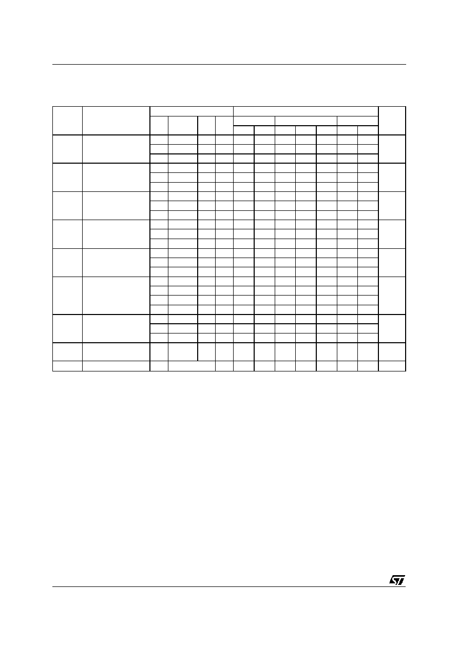
STATIC ELECTRICAL CHARACTERISTICS (over recommended operating conditions, voltages
References to V
SS
)
Symb ol
Parameter
T est Cond it ios
Valu e
Un it
V
I
(V)
V
O
(V)
| I
O
|
(
µ
A)
V
DD
(V)
-40
o
C
25
o
C
85
o
C
Mi n. Max. Min. T yp. Max. Min . Max.
I
L
Quiescent Current
0/5
5
20
0.04
20
150
µ
A
0/10
10
40
0.04
40
300
0/15
15
80
0.04
80
600
V
OH
Output High
Voltage
0/5
< 1
5
4.95
4.95
4.95
V
0/10
< 1
10
9.95
9.95
9.95
0/15
< 1
15
14.95
14.95
14.95
V
OL
Output Low
Voltage
5/0
< 1
5
0.05
0.05
0.05
V
10/0
< 1
10
0.05
0.05
0.05
15/0
< 1
15
0.05
0.05
0.05
V
IH
Input High
Voltage
0.5/4.5
< 1
5
3.5
3.5
3.5
V
1/9
< 1
10
7
7
7
1.5/13.5
< 1
15
11
11
11
V
IL
Input Low
Voltage
4.5/0.5
< 1
5
1.5
1.5
1.5
V
9/1
< 1
10
3
3
3
13.5/1.5
< 1
15
4
4
4
I
OH
Output Drive
Current
0/5
2.5
5
-1.53
-1.36
-3.2
-1.1
mA
0/5
4.6
5
-0.52
-0.44
-1
-0.36
0/10
9.5
10
-1.3
-1.1
-2.6
-0.9
0/15
13.5
15
-3.5
-3.0
-6.8
-2.4
I
OL
Output Sink Current
0/5
0.4
5
0.52
0.44
1
0.36
mA
0/10
0.5
10
1.3
1.1
2.6
0.9
0/15
1.5
15
3.6
3.0
6.8
2.4
I
IH
, I
IL
Input Leakage
Current
0/18 Any Input
18
±
0.1
±
10
-5
±
0.1
±
1
µ
A
C
I
Input Capacitance
Any Input
5
7.5
pF
TheNoise Margin for both "1" and "0" level is: 1V min.withV
DD
= 5 V, 2 V min.with V
DD
= 10 V, 2.5 V min. with V
DD
= 15 V
HCF4521
4/12

DYNAMIC ELECTRICAL CHARACTERISTICS (T
amb
= 25
o
C, C
L
= 50 pF, R
L
= 200 K
,
typical temperaturecoefficent for all V
DD
values is 03 %/
o
C, all input rise and fall times= 20 ns)
Symb ol
Parameter
T est Cond ition s
Value
Un it
V
DD
(V)
Min.
Typ.
Max.
t
PLH
Output Rise Time
5
100
200
ns
10
50
100
15
40
80
t
PHL
Output Fall Time
5
100
200
ns
10
50
100
15
40
80
t
PHL
t
PLH
Propagation Delay Time Clock to Q18
5
4.5
9.0
µ
s
10
1.7
3.5
15
1.3
2.7
t
PHL
t
PLH
Propagation Delay Time Clock to Q24
5
6.0
12
µ
s
10
2.2
4.5
15
1.7
3.5
t
PHL
Propagation Delay Time RESET to Qn
5
1300
2600
ns
10
500
1000
15
375
750
t
WH(cl)
Clock Pulse Width
5
385
140
ns
10
150
55
15
120
40
f
cl
Clock Pulse Frequency
5
3.5
2
MHz
10
9
5
15
12
6.5
t
TLH
t
THL
Clock Rise and Fall Time
5
15
µ
s
10
15
15
15
t
W(R)
Reset Pulse Width
5
1400
700
ns
10
600
300
15
450
225
HCF4521
5/12