1/12
October 2002
s
HIGH NOISE IMMUNITY
s
VOLTAGE SUPPLY RANGE 3V TO 18V
s
ALL STAGE ARE PRESETTABLE
s
RESET DISABLES THE RC OSCILLATOR
FOR LOW STANDBY POWER DRAIN
s
RC AND CRYSTAL OSCILLATOR OUTPUT
ARE CAPABLE OF DRIVING EXTERNAL
LOADS
s
QUIESCENT CURRENT SPECIF. UP TO 20V
s
5V, 10V AND 15V PARAMETRIC RATINGS
s
INPUT LEAKAGE CURRENT
I
I
= 100nA (MAX) AT V
DD
= 18V T
A
= 25°C
s
100% TESTED FOR QUIESCENT CURRENT
s
MEETS ALL REQUIREMENTS OF JEDEC
JESD13B "STANDARD SPECIFICATIONS
FOR DESCRIPTION OF B SERIES CMOS
DEVICES"
DESCRIPTION
HCF4521B is a monolithic integrated circuit
fabricated in Metal Oxide Semiconductor
technology available in DIP and SOP packages.
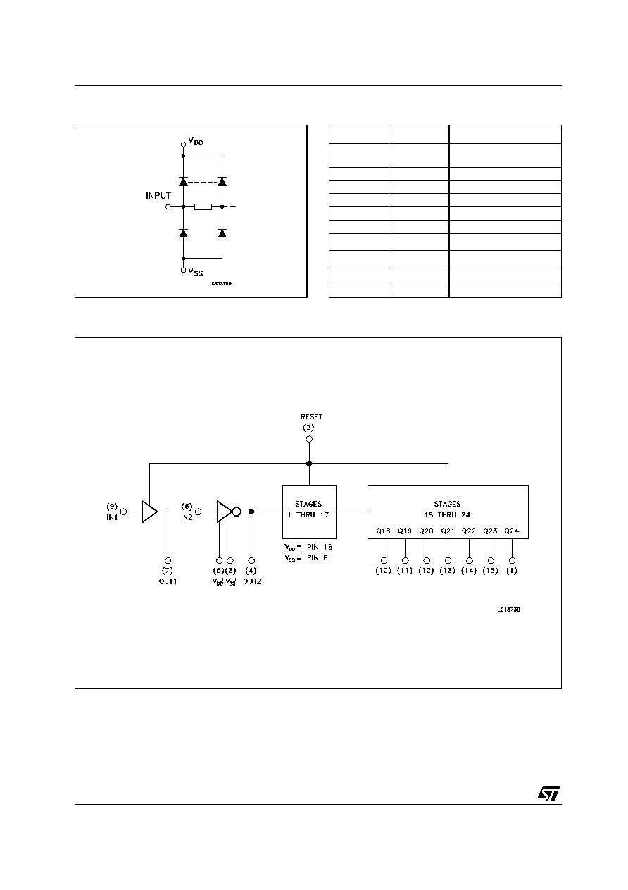
HCF4521B has a chain of 24 flip-flops with an
input circuit that allows three modes of operation.
The input circuit functions as a crystal or RC
oscillator or as an input buffer for an external
oscillator. Each flip-flop preforms a divide-by-two
function giving a total count of 2
24
= 16,777,216.
The count advances on the negative going edge
of the clock. Access is available to the final seven
stages giving the device added flexibility.
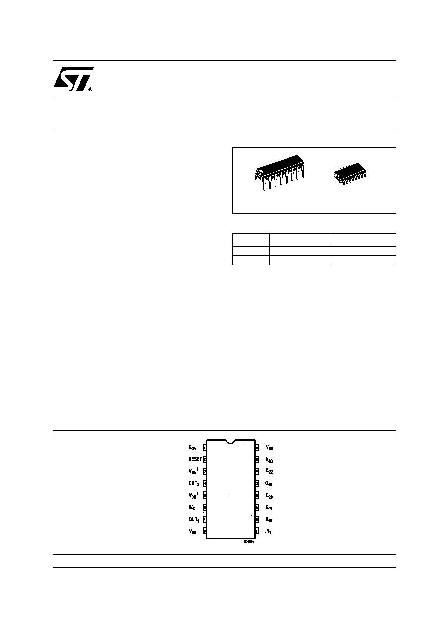
HCF4521B
24-STAGE FREQUENCY DIVIDER
PIN CONNECTION
ORDER CODES
PACKAGE
TUBE
T & R
DIP
HCF4521BEY
SOP
HCF4521BM1
HCF4521M013TR
DIP
SOP
HCF4521B
3/12
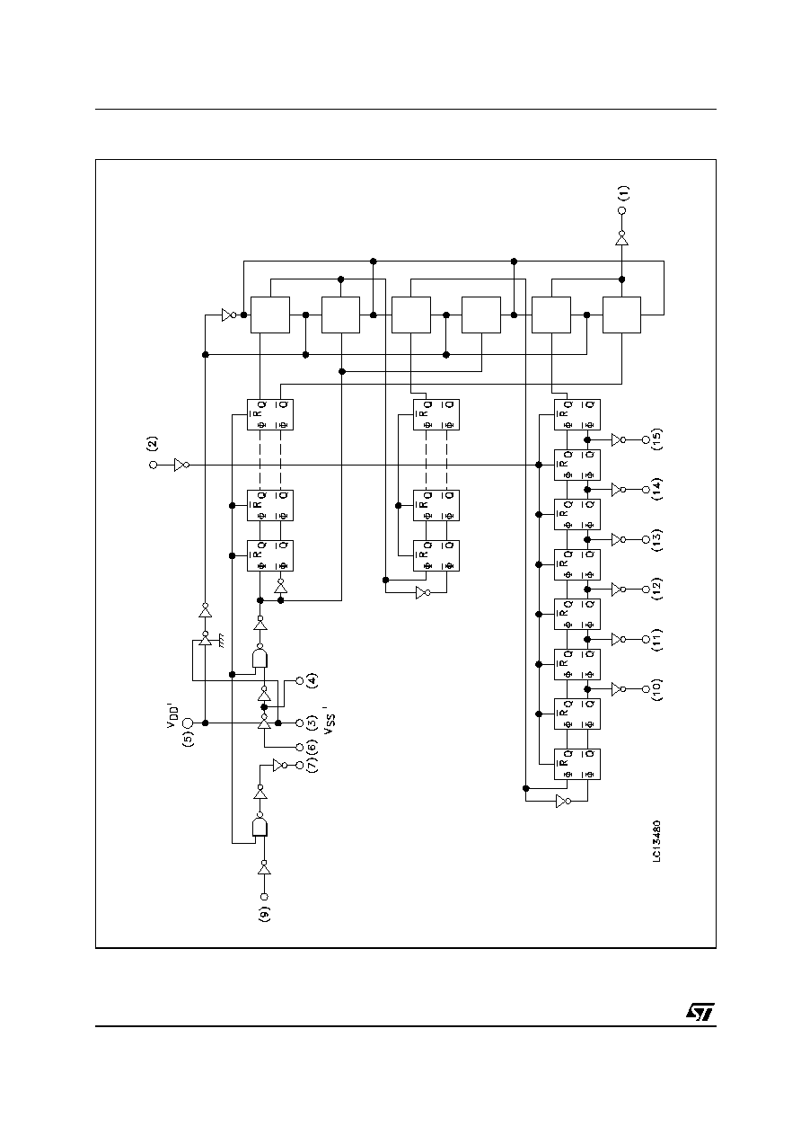
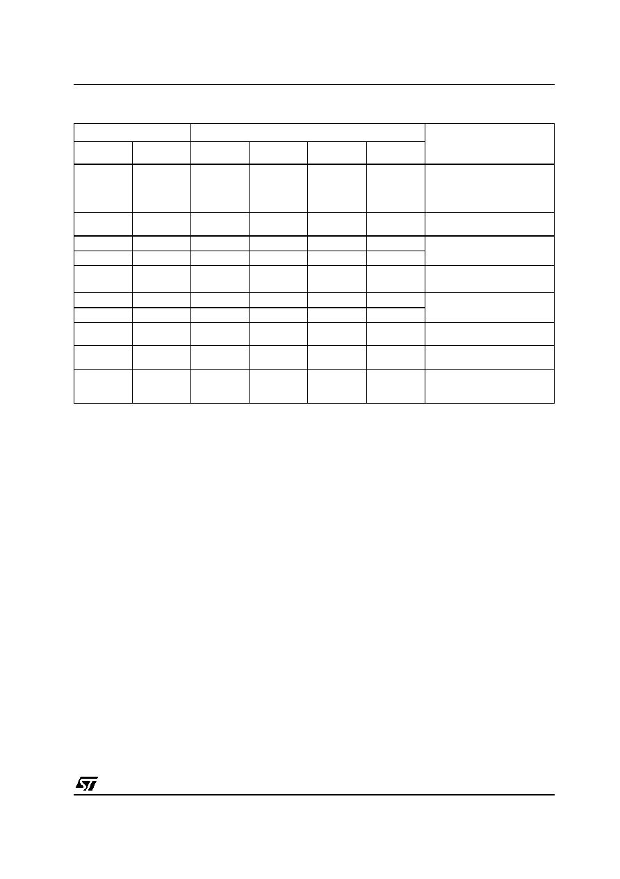
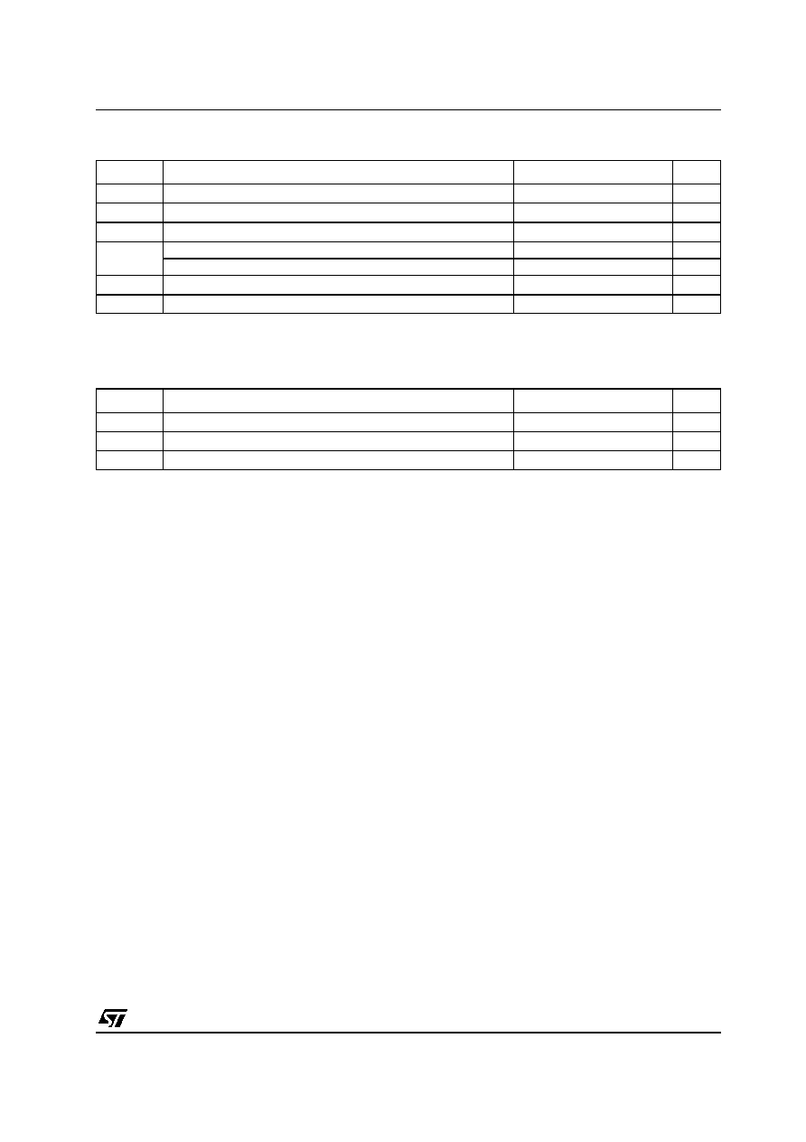
FUNCTIONAL TEST SEQUENCE
A test function (see Functional Test Circuit) has been included for the reduction of test time required to exercise all 24 counter stages. This
test function divides the counter into three 8-stage sections and 255 counts are loaded in each of the 8-stage sections in parallel. All flip-flop
are now at a logic "1". The counter in now returned to the normal 24-stages in series configuration. One more pulse is entered into Input 2
(In2) which will cause the counter to ripple from an all "1" state to an all "0" state.
INPUTS
OUTPUTS
COMMENTS
RESET
IN 2
OUT
V
SS
1
V
DD
1
Q18 - Q24
H
L
L
V
DD
V
SS
L
Counter is in three 8-stage
sections in parallel mode
Counter in reset. IN 2 and
OUT 2 are tied together
L
H
H
V
DD
V
SS
L
First LOW-to-HIGH transition
at IN 2
L
L
L
V
DD
V
SS
L
255 LOW-to-HIGH transition
are clocked in at IN 2
L
H
H
V
DD
V
SS
L
L
H
H
V
DD
V
SS
H
The 255th LOW-to-HIGH
transition
L
L
L
V
DD
V
SS
H
L
L
L
V
SS
V
SS
H
L
H
L
V
SS
V
DD
H
Counter Converted Back to
24-Stage in Series Mode
L
H
L
V
SS
V
DD
H
OUT 2 reverts to output opera-
tion
L
L
H
V
SS
V
DD
L
Counter ripples from an
all-HIGH state to an all-LOW
state
HCF4521B
5/12
ABSOLUTE MAXIMUM RATINGS
Absolute Maximum Ratings are those values beyond which damage to the device may occur. Functional operation under these conditions is
not implied.
All voltage values are referred to V
SS
pin voltage.
RECOMMENDED OPERATING CONDITIONS
Symbol
Parameter
Value
Unit
V
DD
Supply Voltage
-0.5 to +22
V
V
I
DC Input Voltage
-0.5 to V
DD
+ 0.5
V
I
I
DC Input Current
±
10
mA
P
D
Power Dissipation per Package
200
mW
Power Dissipation per Output Transistor
100
mW
T
op
Operating Temperature
-55 to +125
°C
T
stg
Storage Temperature
-65 to +150
°C
Symbol
Parameter
Value
Unit
V
DD
Supply Voltage
3 to 20
V
V
I
Input Voltage
0 to V
DD
V
T
op
Operating Temperature
-55 to 125
°C