 | –≠–ª–µ–∫—Ç—Ä–æ–Ω–Ω—ã–π –∫–æ–º–ø–æ–Ω–µ–Ω—Ç: HCF4527B | –°–∫–∞—á–∞—Ç—å:  PDF PDF  ZIP ZIP |

HCC4527B
HCF4527B
September 1990
BCD RATE MULTIPLEXER
EY
(Plastic Package)
DESCRIPTION
ORDER CODES :
HCC4076BF
HCF4076BEY
HCF4076BC1
F
(Ceramic Package)
C1
(Chip Carrier)
PIN CONNECTIONS
The HCC4527B (extended temperature range) and
HCF4527B (intermediate temperature range) are
monolithic integrated circuit, available in 16-lead
dual in line plastic or ceramic package.
The HCC/HCF4527B is a low power 4 bit digital rate
multiplier that provides an output pulse rate which is
the clock input pulse rate multiplied by 1/10 times the
BCD input. For example, when the BCD input is 8,
there will be 8 output pulses for every 10 input
pulses. This device may be used to preform arith-
metic operations (add, subtract, divide, raise to a
power), solve algebraic and differential equations,
generate naturel logarithms and trigonometric func-
.
CASCADABLE IN MULTIPLES OF 4-BITS
.
SET TO 9 INPUT AND 9 DETECT OUTPUT
.
QUIESCENT CURRENT SPECIFIED TO 20V
FOR HCC DEVICE
.
STANDARDIZED
SYMMETRICAL
OUTPUT
CHARACTERISTICS
.
5V, 10V AND 15V PARAMETRIC RATINGS
.
INPUT CURRENT OF 100nA AT 18V AND 25
o
C
FOR HCC DEVICE
.
100% TESTED FOR QUIESCENT CURRENT
.
MEETS ALL REQUIREMENTS OF JEDEC TEN-
TATIVE STANDARD N. 13A, " STANDARD
SPECIFICATIONS FOR DESCRIPTION OF B
SERIES CMOS DEVICES "
1/13

FUNCTIONAL DIAGRAM
ABSOLUTE MAXIMUM RATING
Symbol
Parameter
Value
Unit
V
DD
*
Supply Voltage: HCC Types
HCF Types
-0.5 to +20
-0.5 to +18
V
V
V
i
Input Voltage
-0.5 to V
DD
+ 0.5
V
I
I
DC Input Current (any one input)
±
10
mA
P
tot
Total Power Dissipation (per package)
Dissipation per Output Transistor
for Top = Full Package Temperature Range
200
100
mW
mW
T
op
Operating Temperature: HCC Types
HCF Types
-55 to +125
-40 to +85
o
C
o
C
T
stg
Storage Temperature
-65 to +150
o
C
Stresses above those listed under "Absolute Maximum Ratings" may cause permanent damage to the device. This is a stress ratingonly and functional
operation of the device at these or any other conditions above those indicated in the operational sections of this specification is not implied. Exposure
to absolute maximum rating conditions for external periods may affect device reliability.
* All voltage values are referred to V
SS
pin voltage.
RECOMMENDED OPERATING CONDITIONS
Symbol
Parameter
Value
Unit
V
DD
Supply Voltage: HCC Types
HCF Types
3 to 18
3 to 15
V
V
V
I
Input Voltage
0 to V
DD
V
T
op
Operating Temperature: HCC Types
HCF Types
-55 to +125
-40 to +85
o
C
o
C
HCC/HCF4527B
2/13

LOGIC DIAGRAM
HCC/HCF4527B
3/13
TRUTH TABLE
Inputs
Outputs
Number of Pulsed or Logic Level
(0 = Low; 1 = High; X = Don't Care)
Number of Pulses or Output
Logic Level
(L = LOW; H = High)
D
C
B
A
CLK
INH IN
STR
CAS
CLR
SET
OUT
OUT
INH
OUT
"9"
OUT
0
0
0
0
10
0
0
0
0
0
L
H
1
1
0
0
0
1
10
0
0
0
0
0
1
1
1
1
0
0
1
0
10
0
0
0
0
0
2
2
1
1
0
0
1
1
10
0
0
0
0
0
3
3
1
1
0
1
0
0
10
0
0
0
0
0
4
4
1
1
0
1
0
1
10
0
0
0
0
0
5
5
1
1
0
1
1
0
10
0
0
0
0
0
6
6
1
1
0
1
1
1
10
0
0
0
0
0
7
7
1
1
1
0
0
0
10
0
0
0
0
0
8
8
1
1
1
0
0
1
10
0
0
0
0
0
9
9
1
1
1
0
1
0
10
0
0
0
0
0
8
8
1
1
1
0
1
1
10
0
0
0
0
0
9
9
1
1
1
1
0
0
10
0
0
0
0
0
8
8
1
1
1
1
0
1
10
0
0
0
0
0
9
9
1
1
1
1
1
0
10
0
0
0
0
0
8
8
1
1
1
1
1
1
10
0
0
0
0
0
9
9
1
1
X
X
X
X
10
1
0
0
0
0
s
s
H
s
X
X
X
X
10
0
1
0
0
0
L
H
1
1
X
X
X
X
10
0
0
1
0
0
H
q
1
1
1
X
X
X
10
0
0
0
1
0
10
10
H
L
0
X
X
X
10
0
0
0
1
0
L
H
H
L
X
X
X
X
10
0
0
0
0
1
L
H
L
H
q
Output same as the first 16 lines of this truth table (depending on value of A, B, C, D)
s
Depends on internal state of counter.
HCC/HCF4527B
4/13
STATIC ELECTRICAL CHARACTERISTICS (over recommended operating conditions)
Symbol
Parameter
Test Conditios
Value
Unit
V
I
(V)
V
O
(V)
|I
O
|
(
µ
A)
V
DD
(V)
T
LOW
*
25
o
C
T
HIGH
*
Min.
Max.
Min.
Typ.
Max.
Min.
Max.
I
L
Quiescent
Current
HCC
Types
0/5
5
5
0.04
5
150
µ
A
0/10
10
10
0.04
10
300
0/15
15
20
0.04
20
600
0/20
20
100
0.08
100
3000
HCF
Types
0/5
5
20
0.04
20
150
0/10
10
40
0.04
40
300
0/15
15
80
0.04
80
600
V
OH
Output High
Voltage
0/5
< 1
5
4.95
4.95
4.95
V
0/10
< 1
10
9.95
9.95
9.95
0/15
< 1
15
14.95
14.95
14.95
V
OL
Output Low
Voltage
5/0
< 1
5
0.05
0.05
0.05
V
10/0
< 1
10
0.05
0.05
0.05
15/0
< 1
15
0.05
0.05
0.05
V
IH
Input High
Voltage
0.5/4.5
< 1
5
3.5
3.5
3.5
V
1/9
< 1
10
7
7
7
1.5/13.5
< 1
15
11
11
11
V
IL
Input Low
Voltage
4.5/0.5
< 1
5
1.5
1.5
1.5
V
9/1
< 1
10
3
3
3
13.5/1.5
< 1
15
4
4
4
I
OH
Output
Drive
Current
HCC
Types
0/5
2.5
5
-2
-1.6
-3.2
-1.15
mA
0/5
4.6
5
-0.64
-0.51
-1
-0.36
0/10
9.5
10
-1.6
-1.3
-2.6
-0.9
0/15
13.5
15
-4.2
-3.4
-6.8
-2.4
HCF
Types
0/5
2.5
5
-1.53
-1.36
-3.2
-1.1
0/5
4.6
5
-0.52
-0.44
-1
-0.36
0/10
9.5
10
-1.3
-1.1
-2.6
-0.9
0/15
13.5
15
-3.6
-3.0
-6.8
-2.4
I
OL
Output
Sink
Current
HCC
Types
0/5
0.4
5
0.64
0.51
1
0.36
mA
0/10
0.5
10
1.6
1.3
2.6
0.9
0/15
1.5
15
4.2
3.4
6.8
2.4
HCF
Types
0/5
0.4
5
0.53
0.44
1
0.36
0/10
0.5
10
1.3
1.1
2.6
0.9
0/15
1.5
15
3.6
3.0
6.8
2.4
I
IH
, I
IL
Input Leakage
Current
0/18
Any Input
18
±
0.1
±
10
-5
±
0.1
±
1
µ
A
0/15
15
±
0.3
±
10
-5
±
0.3
±
1
µ
A
C
I
Input Capacitance
Any Input
5
7.5
pF
* T
LOW
= -55
o
C for HCC device: -40
o
C for HCF device.
* T
HIGH
= +125
o
C for HCC device: +85
o
C for HCF device.
The Noise Margin for both "1" and "0" level is: 1V min. with V
DD
= 5 V, 2 V min. with V
DD
= 10 V, 2.5 V min. with V
DD
= 15 V
HCC/HCF4527B
5/13

DYNAMIC ELECTRICAL CHARACTERISTICS (T
amb
= 25
o
C, C
L
= 50 pF, R
L
= 200 K
,
typical temperature coefficent for all V
DD
values is 03 %/
o
C, all input rise and fall times= 20 ns)
Symbol
Parameter
Test Conditions
Value
Unit
V
DD
(V)
Min.
Typ.
Max.
t
PLH
t
PHL
Propagation Delay Time
Clock to Output)
5
110
220
ns
10
55
110
15
45
90
t
PLH
t
PHL
Propagation Delay Time
Clock or Strobe to Output
5
150
300
ns
10
75
150
15
60
120
t
PLH
Propagation Delay Time
Clock to Inhibit Output
5
320
640
ns
10
145
290
15
100
200
t
PHL
Propagation Delay Time
Clock to Inhibit Output
5
250
500
ns
10
100
200
15
75
150
t
PLH
t
PHL
Propagation Delay Time
Clear to Output
5
380
760
ns
10
175
550
15
130
260
t
PLH
t
PHL
Propagation Delay Time
Clock to "9" or "1" Q Output
5
300
600
ns
10
125
250
15
90
180
t
PLH
t
PHL
Propagation Delay Time
Cascade to Output
5
90
180
ns
10
45
90
15
35
70
t
PLH
t
PHL
Propagation Delay Time
Inhibit Input to Inhibit Output
5
130
260
ns
10
60
120
15
45
90
t
PLH
t
PHL
Propagation Delay Time
Set to Output
5
330
660
ns
10
150
300
15
110
220
t
THL
t
TLH
Transition Time
5
100
200
ns
10
50
100
15
40
80
f
CL
Maximum Clock Frequency
5
1.2
2.4
MHz
10
2.5
5
15
3.5
7
t
W
Clock Pulse Width
5
330
165
ns
10
170
85
15
100
50
t
r
, t
f
Clock Rise or Fall Time
5
15
µ
s
10
15
15
15
t
W
Set or Clear Pulse Width
5
160
80
ns
10
90
45
15
60
30
t
setup
Inhibit Input Setup Time
5
100
50
ns
10
40
20
15
20
10
HCC/HCF4527B
6/13
DYNAMIC ELECTRICAL CHARACTERISTICS (continued)
Symbol
Parameter
Test Conditions
Value
Unit
V
DD
(V)
Min.
Typ.
Max.
t
R
Inhibit Input Removal Time
5
240
120
ns
10
130
65
15
110
55
t
R
Set Remova Time
5
150
75
ns
10
80
40
15
50
25
t
R
Clear Removal Time
5
60
30
ns
10
40
20
15
30
15
APPLICATION NOTE
For fractional multipliers with more than one digit,
HCC/HCF4527B devices may be cascated in two
different modes: the Add mode and the Mltiply mode
(see figures 1 and 2).
When two units are cascated in Add mode and pro-
grammed to 9 and 4 respectively, the more signifi-
cant unit will have 9 output pulses for every 10 input
pulses and the other unit will have 4 output pulses
for every 100 input pulses for a total of:
9
10
+
4
100
=
94
100
In the multiply mode, the fraction programmed into
the first rate multiplier is multiplied by the fraction
programmed into the second one:
If N
1
= 9 and N
2
= 4
f
out2
=
4
10
f
out1
f
out1
=
9
10
f
clock
f
out2
=
4
10
◊
9
10
f
clock
=
36
100
f
clock
Therefore 36 output pulses for every 100 clock input
pulses.
HCC/HCF4527B
7/13
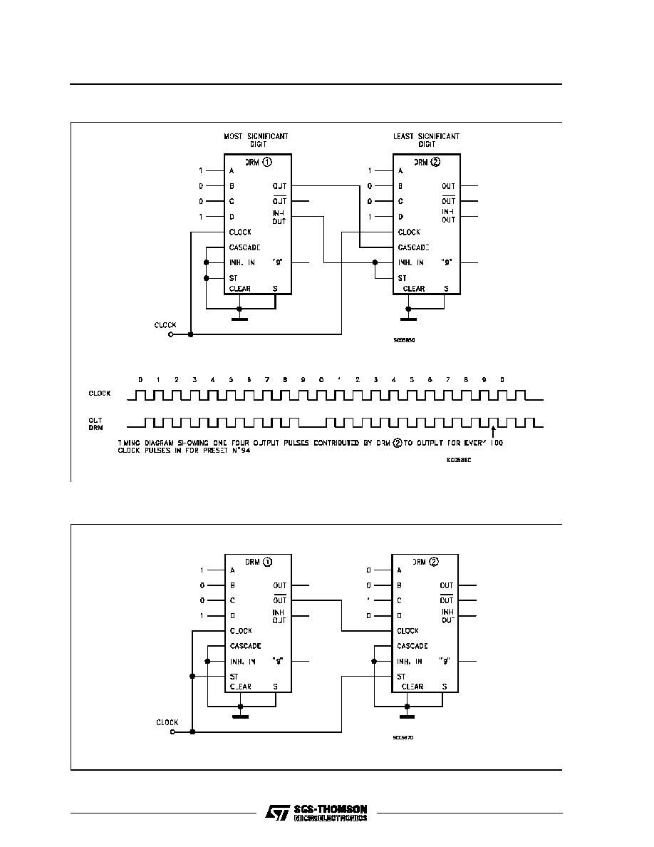
Fig. 2: Two HCC/HCF4527B Cascaded in The "Multiply" Mode With a Preset Number
Fig. 1: Two HCC/HCF4527B Cascaded in The "Add" Mode With a Preset Number
HCC/HCF4527B
8/13
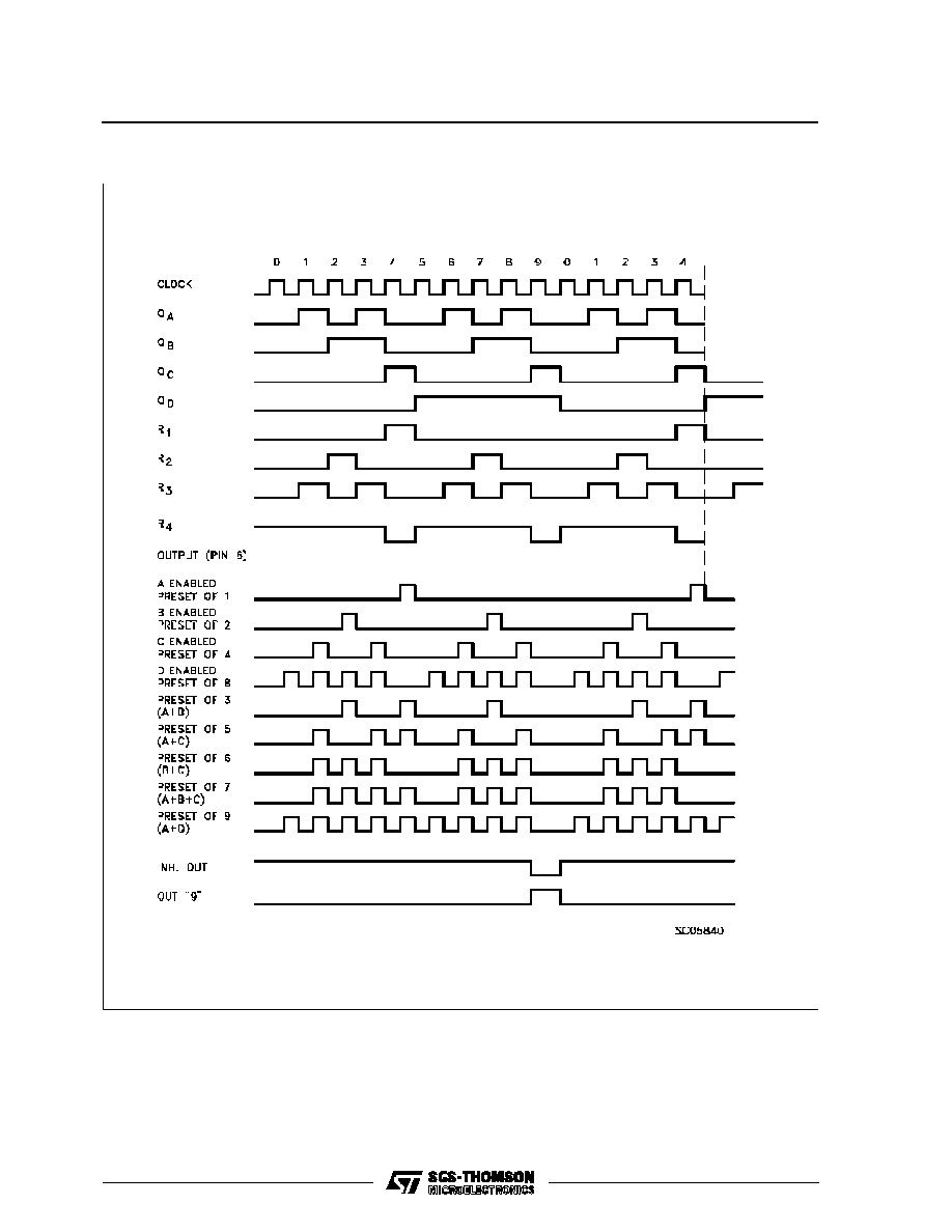
Fig. 3: Timing Diagram (see Logic Diagram)
HCC/HCF4527B
9/13
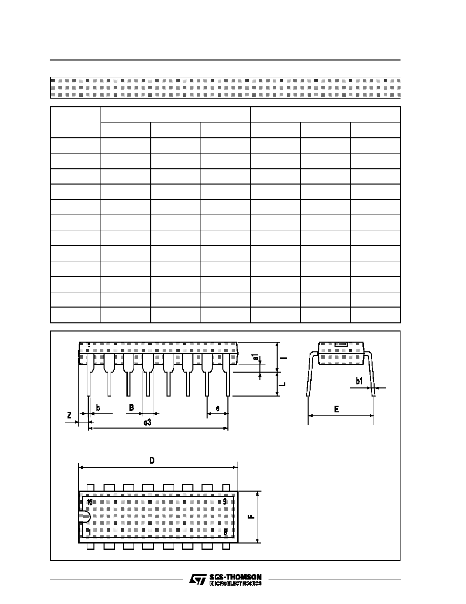
Plastic DIP16 (0.25) MECHANICAL DATA
DIM.
mm
inch
MIN.
TYP.
MAX.
MIN.
TYP.
MAX.
a1
0.51
0.020
B
0.77
1.65
0.030
0.065
b
0.5
0.020
b1
0.25
0.010
D
20
0.787
E
8.5
0.335
e
2.54
0.100
e3
17.78
0.700
F
7.1
0.280
I
5.1
0.201
L
3.3
0.130
Z
1.27
0.050
P001C
HCC/HCF4527B
10/13
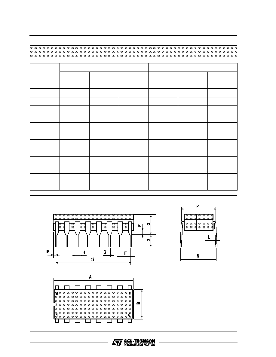
Ceramic DIP16/1 MECHANICAL DATA
DIM.
mm
inch
MIN.
TYP.
MAX.
MIN.
TYP.
MAX.
A
20
0.787
B
7
0.276
D
3.3
0.130
E
0.38
0.015
e3
17.78
0.700
F
2.29
2.79
0.090
0.110
G
0.4
0.55
0.016
0.022
H
1.17
1.52
0.046
0.060
L
0.22
0.31
0.009
0.012
M
0.51
1.27
0.020
0.050
N
10.3
0.406
P
7.8
8.05
0.307
0.317
Q
5.08
0.200
P053D
HCC/HCF4527B
11/13
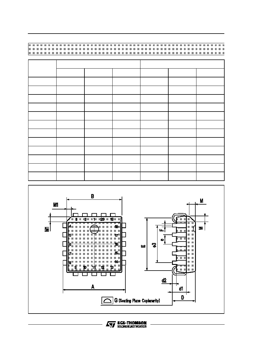
PLCC20 MECHANICAL DATA
DIM.
mm
inch
MIN.
TYP.
MAX.
MIN.
TYP.
MAX.
A
9.78
10.03
0.385
0.395
B
8.89
9.04
0.350
0.356
D
4.2
4.57
0.165
0.180
d1
2.54
0.100
d2
0.56
0.022
E
7.37
8.38
0.290
0.330
e
1.27
0.050
e3
5.08
0.200
F
0.38
0.015
G
0.101
0.004
M
1.27
0.050
M1
1.14
0.045
P027A
HCC/HCF4527B
12/13

Information furnished is believed to be accurate and reliable. However, SGS-THOMSON Microelectronics assumes no responsability for the
consequences of use of such information nor for any infringement of patents or other rights of third parties which may results from its use. No
license is granted by implication or otherwise under any patent or patent rights of SGS-THOMSON Microelectronics. Specifications mentioned
in this publication are subject to change without notice. This publication supersedes and replaces all information previously supplied.
SGS-THOMSON Microelectronics products are not authorized for use as critical components in life support devices or systems without express
written approval of SGS-THOMSON Microelectonics.
©
1994 SGS-THOMSON Microelectronics - All Rights Reserved
SGS-THOMSON Microelectronics GROUP OF COMPANIES
Australia - Brazil - France - Germany - Hong Kong - Italy - Japan - Korea - Malaysia - Malta - Morocco - The Netherlands -
Singapore - Spain - Sweden - Switzerland - Taiwan - Thailand - United Kingdom - U.S.A
HCC/HCF4527B
13/13