 | –≠–ª–µ–∫—Ç—Ä–æ–Ω–Ω—ã–π –∫–æ–º–ø–æ–Ω–µ–Ω—Ç: HCF4536B | –°–∫–∞—á–∞—Ç—å:  PDF PDF  ZIP ZIP |
HCC/HCF4536B
PROGRAMMABLE TIMER
.
24 FLIP-FLOP STAGES - COUNTS FROM
2
0
TO 2
24
.
LAST 16 STAGES SELECTABLE BY BCD SE-
LECT CODE
.
BYPASS INPUT ALLOWS BYPASSING FIRST
8 STAGES
.
ON-CHIP RC OSCILLATOR PROVISION
.
CLOCK INHIBIT INPUT
.
SCHMITT-TRIGGER IN CLOCK LINE PER-
MITS OPERATION WITH VERY LONG RISE
AND FALL TIMES
.
ON-CHIP MONOSTABLE OUTPUT PROVI-
SION
.
TYPICAL f
CL
= 3MHz AT V
DD
= 10V
.
TEST MODE ALLOWS FAST TEST SE-
QUENCE
.
SET AND RESET INPUTS
.
CAPABLE OF DRIVING TWO LOW POWER
TTL
LOADS,
ONE
LOWER-POWER
SCHOTTKY LOAD, OR TWO HTL LOADS
OVER THE RATED TEMPERATURE RANGE
.
STANDARDIZED, SYMMETRICAL OUTPUT
CHARACTERISTICS
.
QUIESCENT CURRENT AT 20V FOR HCC DE-
VICE
.
5V, 10V, AND 15V PARAMETRIC RATINGS
.
INPUT CURRENT OF 100 nA AT 18V AND 25
∞
C
FOR HCC DEVICE
.
100% TESTED FOR QUIESCENT CURRENT
.
MEETS ALL REQUIREMENTS OF JEDEC TEN-
TATIVE STANDARD N
o
. 13A, "STANDARD
SPECIFICATIONS FOR DESCRIPTION OF "B"
SERIES CMOS DEVICES"
November 1996
DESCRIPTION
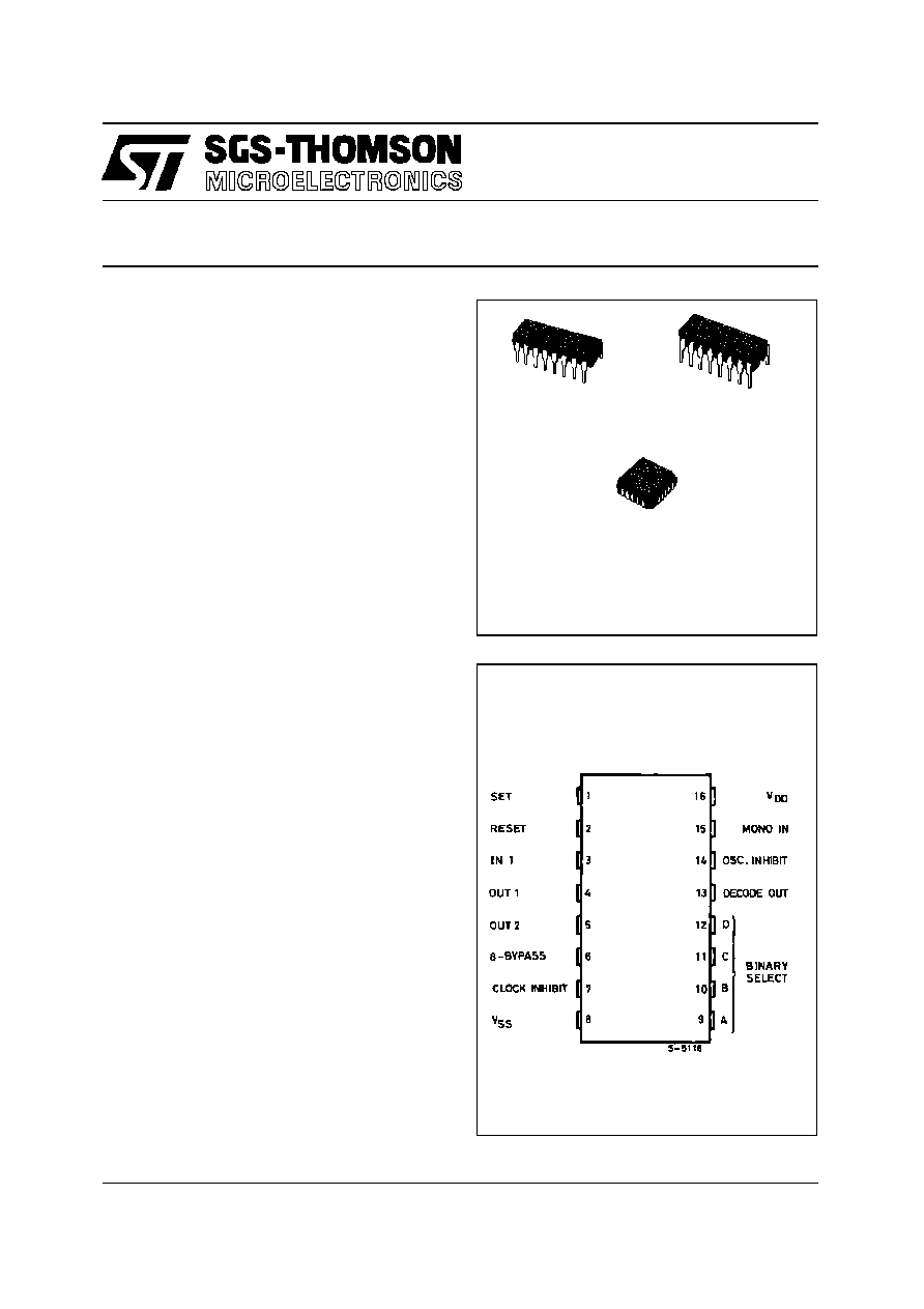
The HCC4536B (extended temperature range) and
HCF4536B (intermediate temperature range) are
monolithic integrated circuits, available in 16-lead
dual in-line plastic or ceramic package. The
HCC/HCF4536B is a programmable timer consi-
sting of 24 ripple-binary counter stages. The salient
feature of this device is its flexibility. The device can
count from 1 to 2
24
or the first 8 stages can be by-
passed to allow an output, selectable by a 4-bit co-
de, from any one of the remaining 16 stages. It can
be driven by an external clock or an RC oscillator
that can be constructed using on-chip components.
EY
(Plastic Package)
F
(Ceramic Package)
C1
(Chip Carrier)
ORDER CODES :
HCC4536BF
HCF4536BEY
HCF4536BC1
PIN CONNECTIONS
1/17
FUNCTIONAL DIAGRAM
ABSOLUTE MAXIMUM RATINGS
Symbol
Parameter
Value
Unit
V
DD
*
Supply Voltage : H CC Types
H C F Types
≠ 0.5 to + 20
≠ 0.5 to + 18
V
V
V
i
Input Voltage
≠ 0.5 to V
DD
+ 0.5
V
I
I
DC Input Current (any one input)
±
10
mA
P
t o t
Total Power Dissipation (per package)
Dissipation per Output Transistor
for T
o p
= Full Package-temperature Range
200
100
mW
mW
T
o p
Operating Temperature : H CC Types
H C F Types
≠ 55 to + 125
≠ 40 to + 85
∞
C
∞
C
T
s t g
Storage Temperature
≠ 65 to + 150
∞
C
Stresses above those listed under "Absolute Maximum Ratings" may cause permanent damage to the device. This is a stress rating only and
functional operation of the device at these or any other conditions above those indicated in the operational sections of this specification is not
implied. Exposure to absolute maximum rating conditions for external periods may affect device reliability.
* All voltages are with respect to V
SS
(GND).
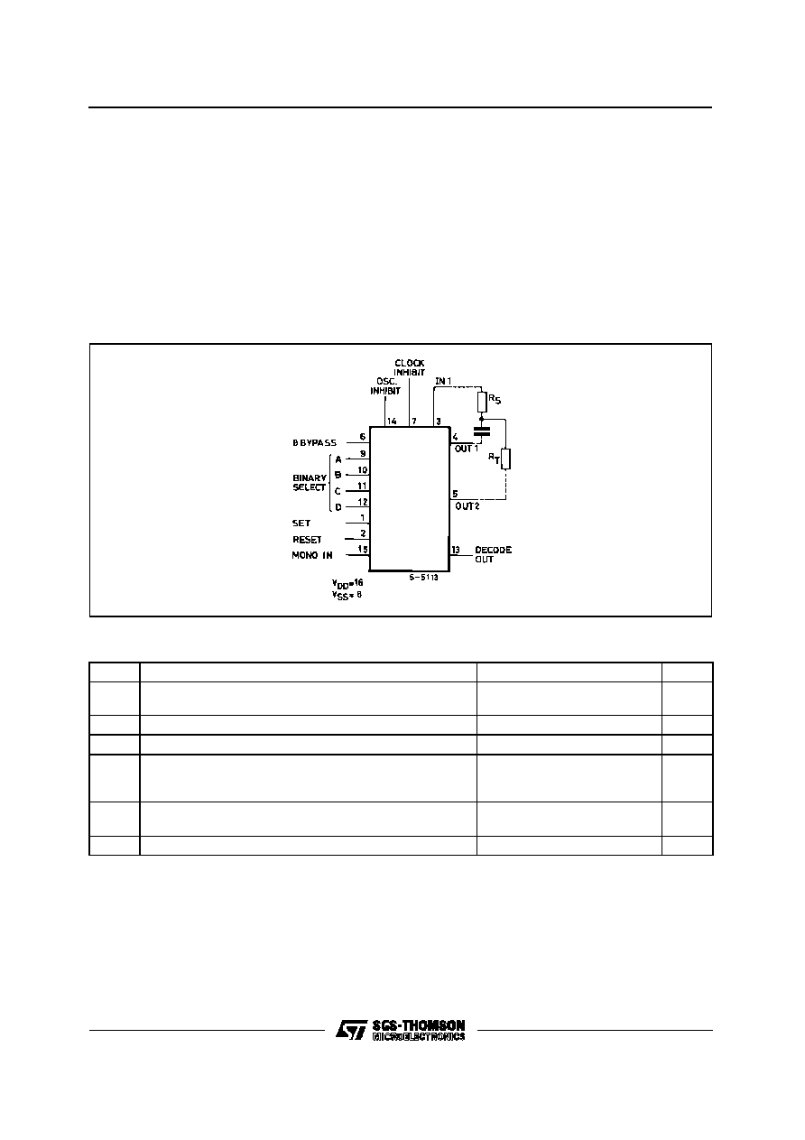
Input IN1 serves as either the external clock input or
the input to the on-chip RC oscillator. OUT1 and
OUT2 are connection terminals for the external RC
components. In addition, an on-chip monostable cir-
cuit is provided to allow a variable pulse width out-
put. Various timing functions can be achieved using
combinations of these capabilities. A logic 1 on the
8-BYPASS input enables a bypass of the first 8 sta-
ges and makes stage 9 the first counter stage of the
last 16 stages. Selection of 1 of 16 outputs is accom-
plished by the decoder and the BCD inputs A, B, C
and D. MONO IN is the timing input for the on-chip
monostable oscillator. Grounding of the MONO IN
terminal through a resistor of 10K
or higher, disa-
bles the one-shot circuit and connects the decoder
directly to the DECODE OUT terminal. A resistor to
V
DD
and a capacitor to ground from the MONO IN
terminal enables the one-shot circuit and controls its
pulse width. A fast test mode is enabled by a logic
1 on 8-BYPASS, SET, and RESET. This mode di-
vides the 24-stage counter into three 8-stage sec-
tions to facilitate a fast test sequence.
HCC/HCF4536B
2/17
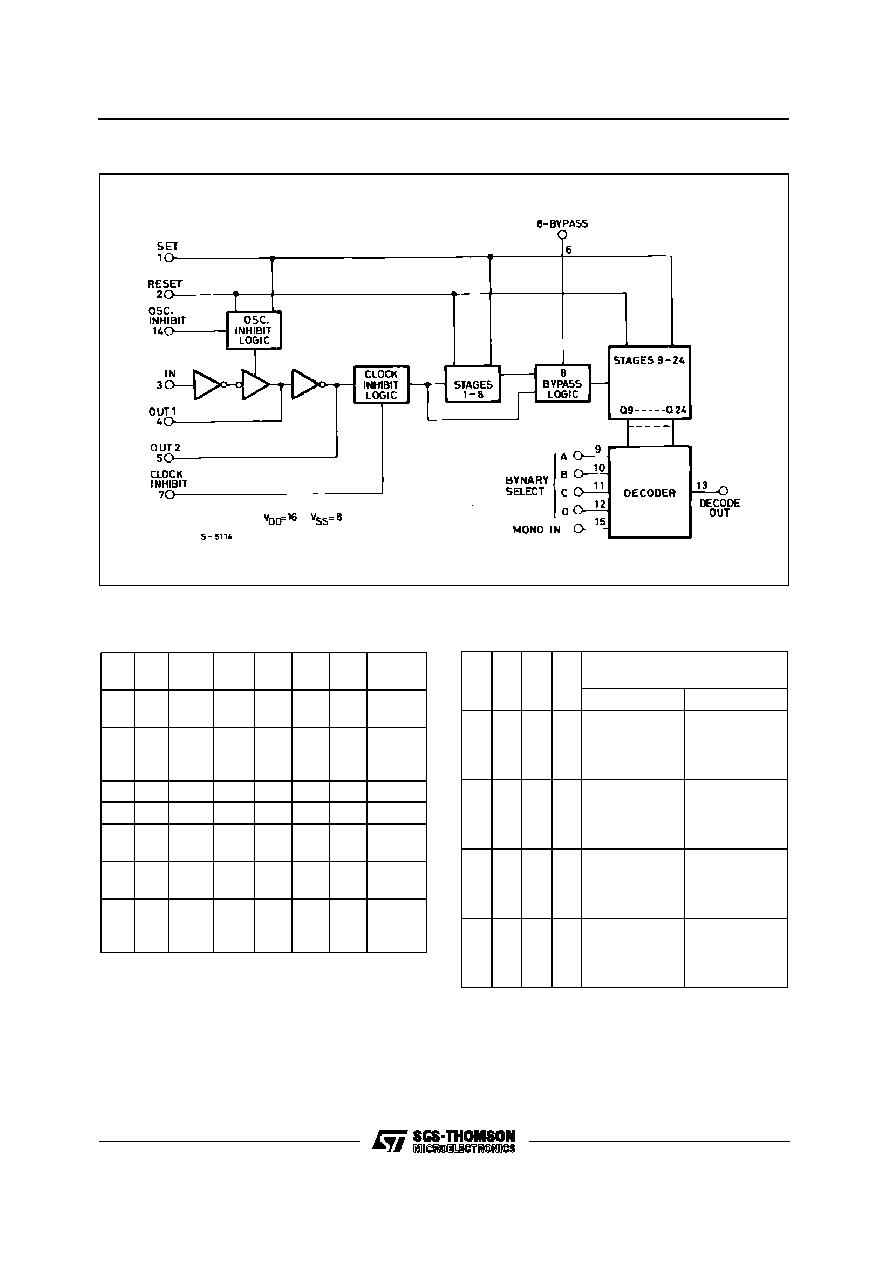
BLOCK DIAGRAM
TRUTH TABLE
I n 1 Set Reset Clock
I n h
Osc
I nh
Out1 Out2 Decode
Out
≠
/
≠
0
0
0
0
≠
/
≠
≠
\≠
No
Change
≠
\≠
0
0
0
0
≠
\≠
≠
/
≠
Advance
to Next
State
X
1
0
0
0
0
1
1
X
0
1
0
0
0
1
0
X
0
0
1
0
No
Change
0
0
0
0
X
0
1
No
Change
1
0
0
0
≠
/
≠
≠
\≠
≠
/
≠
Advance
to Next
State
DECODE OUT SELECTION TABLE
Number or Stages
I n Divider Chai n
D
C
B
A
8-BYPASS = 0 8-BYPASS = 1
0
0
0
0
0
0
0
0
0
0
1
1
0
1
0
1
9
10
11
12
1
2
3
4
0
0
0
0
1
1
1
1
0
0
1
1
0
1
0
1
13
14
15
16
5
6
7
8
1
1
1
1
0
0
0
0
0
0
1
1
0
1
0
1
17
18
19
20
9
10
11
12
1
1
1
1
1
1
1
1
0
0
1
1
0
1
0
1
21
22
23
24
13
14
15
16
0 = Low Level
0 = Low Level
HCC/HCF4536B
3/17
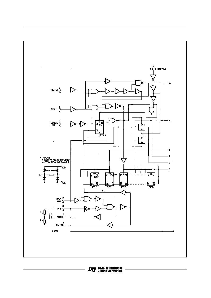
LOGIC DIAGRAMS (continued on next page)
HCC/HCF4536B
4/17
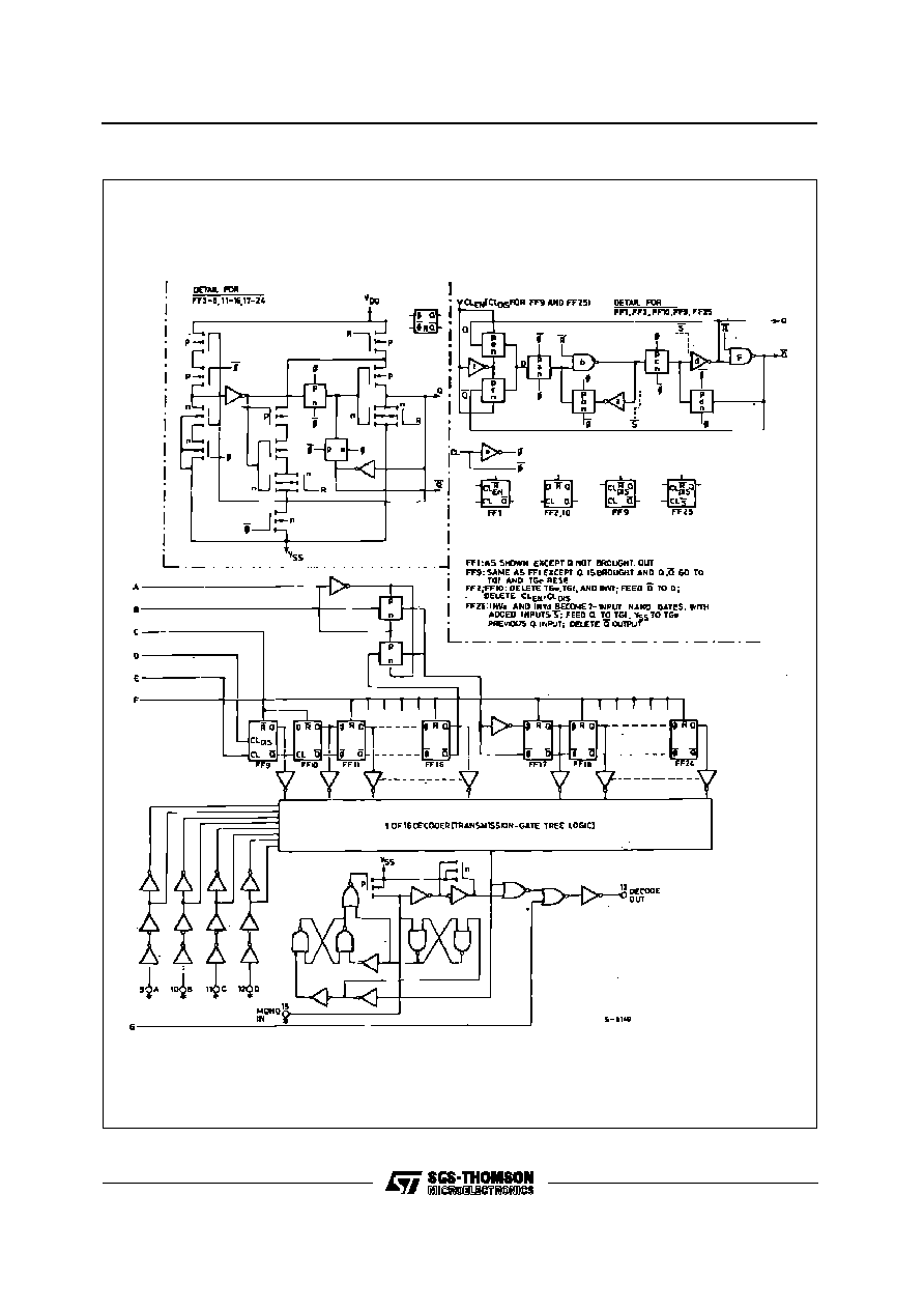
LOGIC DIAGRAMS (continued)
HCC/HCF4536B
5/17
STATIC ELECTRICAL CHARACTERISTICS (over recommended operating conditions)
Test Conditions
Value
V
I
V
O
|I
O
|
V
D D
T
L o w
*
25
∞
C
T
Hi g h
*
Symbol
Parameter
(V)
(V)
(
µ
A)
(V)
Min. Max. Min. Typ. Max. Min. Max.
Unit
I
L
Quiescent
Current
HCC
Types
0/ 5
5
5
0.04
5
150
µ
A
0/10
10
10
0.04
10
300
0/15
15
20
0.04
20
600
0/20
20
100
0.08
100
3000
HCF
Types
0/ 5
5
20
0.04
20
150
0/10
10
40
0.04
40
300
0/15
15
80
0.04
80
600
V
O H
Output High
Voltage
0/ 5
< 1
5
4.95
4.95
4.95
V
0/10
< 1
10
9.95
9.95
9.95
0/15
< 1
15
14.95
14.95
14.95
V
O L
Output Low
Voltage
5/0
< 1
5
0.05
0.05
0.05
V
10/0
< 1
10
0.05
0.05
0.05
15/0
< 1
15
0.05
0.05
0.05
V
IH
Input High
Voltage
0.5/4.5
< 1
5
3.5
3.5
3.5
V
1/9
< 1
10
7
7
7
1.5/13.5
< 1
15
11
11
11
V
IL
Input Low
Voltage
4.5/0.5
< 1
5
1.5
1.5
1.5
V
9/1
< 1
10
3
3
3
13.5/1.5
< 1
15
4
4
4
I
O H
Output
Drive
Current
HCC
Types
0/ 5
2.5
5
≠ 2
≠ 1.6 ≠ 3.2
≠ 1.15
mA
0/ 5
4.6
5
≠ 0.64
≠ 0.51 ≠ 1
≠ 0.36
0/10
9.5
10
≠ 1.6
≠ 1.3 ≠ 2.6
≠ 0.9
0/15
13.5
15
≠ 4.2
≠ 3.4 ≠ 6.8
≠ 2.4
HCF
Types
0/ 5
2.5
5
≠ 1.53
≠ 1.36 ≠ 3.2
≠ 1.1
0/ 5
4.6
5
≠ 0.52
≠ 0.44 ≠ 1
≠ 0.36
0/10
9.5
10
≠ 1.3
≠ 1.1 ≠ 2.6
≠ 0.9
0/15
13.5
15
≠ 3.6
≠ 3.0 ≠ 6.8
≠ 2.4
I
O L
Output
Sink
Current
HCC
Types
0/ 5
0.4
5
0.64
0.51
1
0.36
mA
0/10
0.5
10
1.6
1.3
2.6
0.9
0/15
1.5
15
4.2
3.4
6.8
2.4
HCF
Types
0/ 5
0.4
5
0.52
0.44
1
0.36
0/10
0.5
10
1.3
1.1
2.6
0.9
0/15
1.5
15
3.6
3.0
6.8
2.4
I
IH
, I
IL
Input
Leakage
Current
HCC
Types
0/18
Any Input
18
±
0.1
±
10
≠ 5
±
0.1
±
1
µ
A
HCF
Types
0/15
15
±
0.3
±
10
≠ 5
±
0.3
±
1
C
I
Input Capacitance
Any Input
5
7.5
pF
* T
Low
= ≠ 55
∞
C for HCC device : ≠ 40
∞
C for HCF device.
* T
High
= + 125
∞
C for HCC device : + 85
∞
C for HCF device.
The Noise Margin for both "1" and "0" level is : 1V min. with V
DD
= 5V , 2V min. with V
DD
= 10V, 2.5 V min. with V
DD
= 15V.
HCC/HCF4536B
6/17
DYNAMIC ELECTRICAL CHARACTERISTICS (T
amb
= 25
o
C, C
L
= 50 pF, R
L
= 200 K
,
typical temperature coefficent for all V
DD
values is 03 %/
o
C, all input rise and fall times= 20 ns)
Symbol
Parameter
Test Conditions
Value
Unit
V
DD
(V)
Min.
Typ.
Max.
t
PLH
t
PHL
Propagation Delay Time
Clock to Q1, 8-bypass High
5
1
2
µ
s
10
0.5
1
15
0.35
0.7
Clock to Q1, 8-bypass Low
5
2.5
5
µ
s
10
0.8
1.6
15
0.6
1.2
Clock to Q16
5
4
8
µ
s
10
1.5
3
15
1
2
Q
n
to Q
n + 1
5
150
300
ns
10
75
150
15
50
100
t
PLH
Propagation Delay Time
5
300
600
ns
10
125
250
15
80
160
t
PHL
Reset to Qn
5
3
6
µ
s
10
1
2
15
0.75
1.5
t
TLH
t
THL
Transition Time
5
100
200
ns
10
50
100
15
40
80
t
W
Pulse Width
Clock
5
200
400
ns
10
75
150
15
50
100
Set
5
200
400
ns
10
100
200
15
60
120
Reset
5
3
6
µ
s
10
1
2
15
0.75
1.5
Recovery Time
Set
5
2.5
5
µ
s
10
1
2
15
0.6
1.6
Reset
5
3.5
7
µ
s
10
1.5
3
15
1
2
t
r
, t
f
Clock Input Rise or Fall Time
5
Unlimted
µ
s
10
15
f
CL
Maximum Clock Input Frequency
0.5
1
MHz
10
1.5
3
15
2.5
5
HCC/HCF4536B
7/17

Output Low (sink) Current Characteristics.
Output High (source) Current Characteristics.
Typical Transition Time vs. Load Capacitance.
Typical Propagation Delay Time vs. Load Capacit-
ance (clock to Q1, 8 Bypass high).
Typical Propagation Delay Time vs. Load Capacit-
ance (Clock to Q16, 8 Bypass high).
Typical Propagation Delay Time vs. Load Capacit-
ance (Clock to Q1, 8 Bypass low).
HCC/HCF4536B
8/17
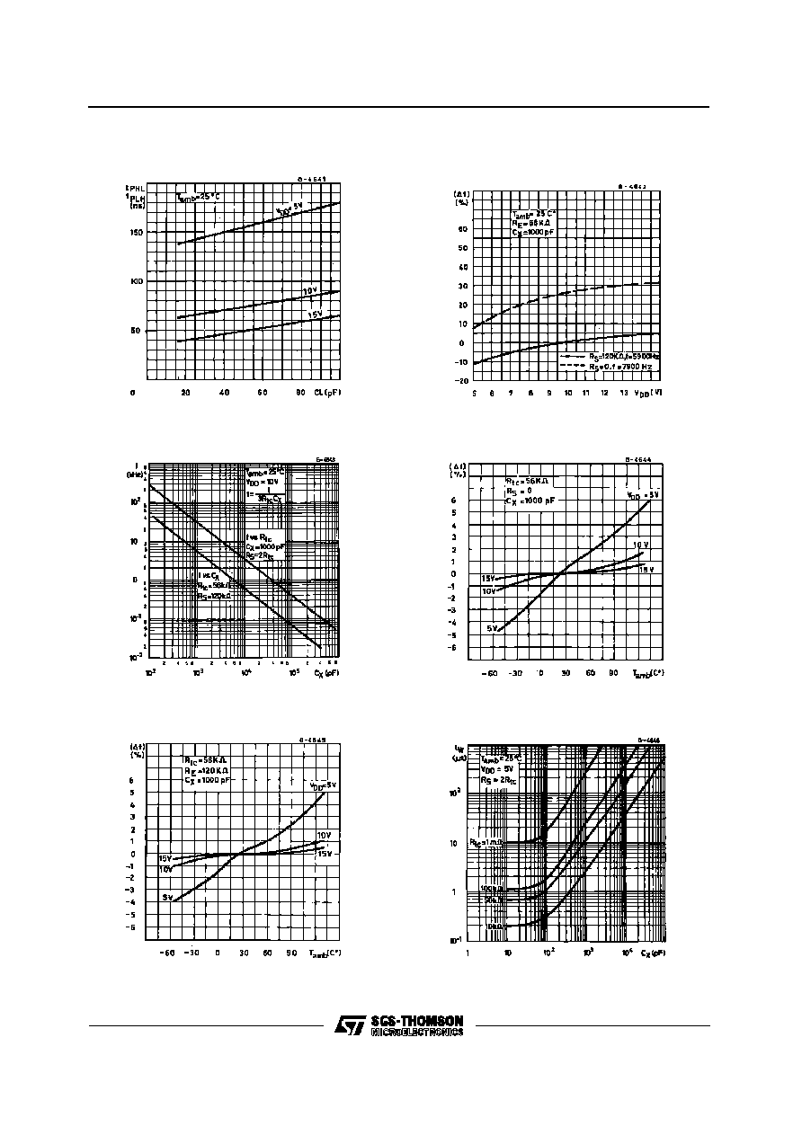
Typical Propagation Delay Time vs. Load Capacit-
ance (Q
N
to Q
N+1
).
Typical RC Oscillator Frequency Deviation vs.
Supply Voltage.
Typical RC Oscillator Frequency Deviation vs.
Time Constant Resistance and Capacitance.
Typical RC Oscillator Frequency Deviation vs. Am-
bient Temperature (R
S
= 0)
.
Typical Pulse Width vs. External Capacitance
(V
DD
= 5V).
Typical RC Oscillator Frequency Deviation vs. Am-
bient Temperature (R
S
= 120K
).
HCC/HCF4536B
9/17

Typical Pulse Width vs. External Capacitance
(V
DD
= 10V).
Typical
Pulse Width vs. External
Capacitance
(V
DD
= 15V).
Typical Dynamic Power Dissipation vs. Input
Pulse Frequency.
TYPICAL APPLICATIONS
Time Internal Configuration Using External Clock
; Set and Clock Inhibit Functions.
Time Internal Configuration Using External Clock
; Reset and Output Monostable to Achieve a
Pulse Output.
HCC/HCF4536B
10/17
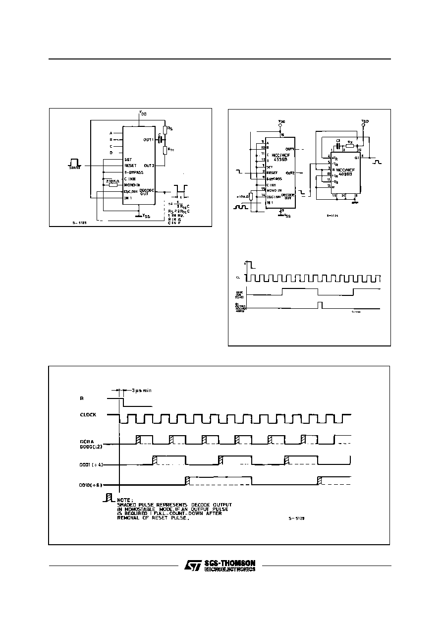
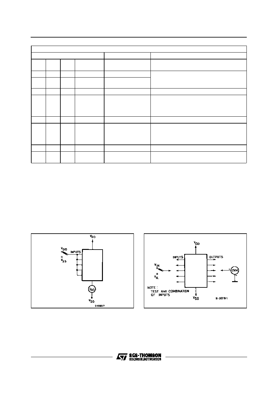
Time Internal Configuration Using Onchip RC Os-
cillator and Reset Input to Initiate Time Interval.
Application Showing Use of 4098B and 4536B to
get Decode Pulse 8 Clock Pulses after Reset
TYPICAL APPLICATIONS (Continued)
TIMING DIAGRAM
HCC/HCF4536B
11/17
Functional Test Sequence
Inputs
Outputs
Comments
I n1
Set
Reset
8-Bypass
Decade Out
Q 1 Thru Q 2 4
All 2 4 steps a r e in reset mode.
1
0
1
1
0
1
1
1
1
0
Counter is in three 8-stage section in parallel
mode.
0
1
1
1
0
First "1" to "0" Transition of Clock
1
0
≠
≠
1
1
1
255 "1" to "0" transitions are clocked in the
counter.
0
1
1
1
1
The 255 "1" to "0" Transition
0
0
0
0
1
Counter converted back to 24 stages in series
mode.
Set and Reset must be connected together and
simultaneoulsy go from "1" to "0".
1
0
0
0
1
In
1
switches to a "1".
0
0
0
0
0
Counter Ripples from an all "1" state to an all "0"
state.
Input Voltage.
Quiescent Device Current.
TEST CIRCUITS
FUNCTIONAL TEST SEQUENCE
Test Function has been included for the reduction of
test time required to exercise all 24 counter stages.
This test function divides the counter into three 8-
stage section and 255 counts are loaded in each of
the 8-stage sections in parallel. All flip-flops are now
at a "1". The counter is now returned to the normal
24-steps in series configuration. One more pulse is
entered into In
1
which will cause the counter to ripple
from an all "1" state to an all "0" state.
HCC/HCF4536B
12/17
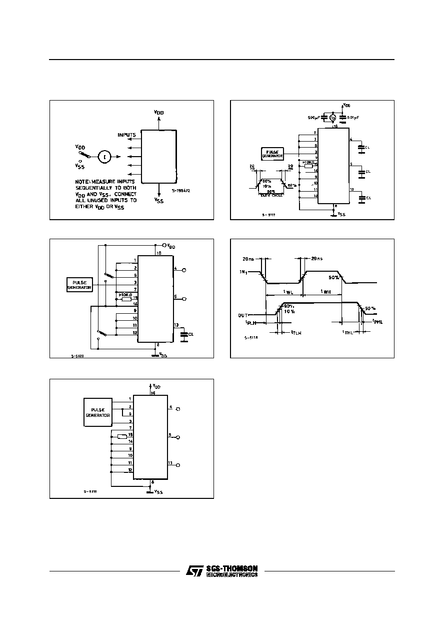
Dynamic Power Dissipation.
Switching Time.
Input Leakage Current.
Input Waveforms for Switching-Time.
TEST CIRCUITS (continued)
Functional.
HCC/HCF4536B
13/17
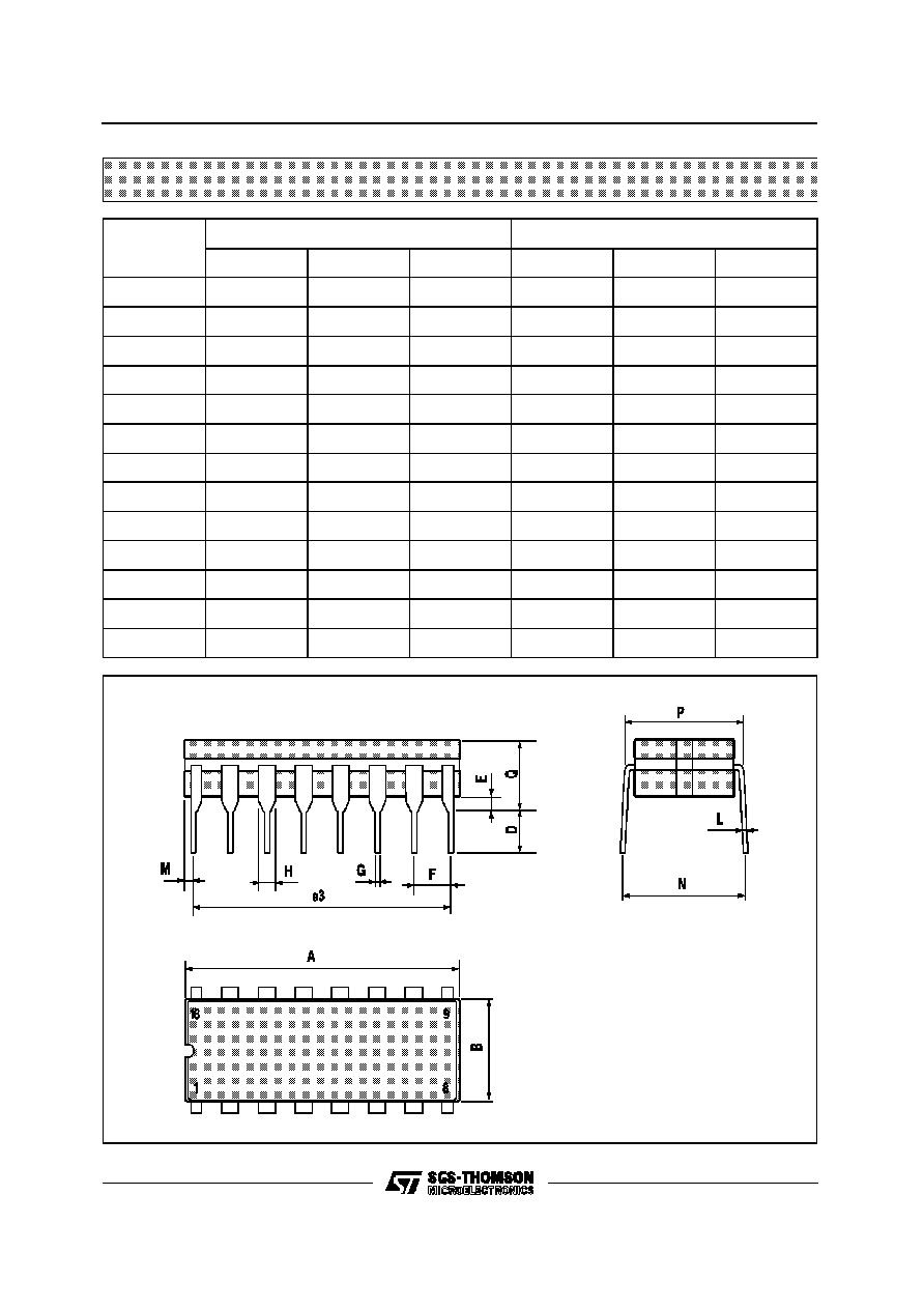
Plastic DIP16 (0.25) MECHANICAL DATA
DIM.
mm
inch
MIN.
TYP.
MAX.
MIN.
TYP.
MAX.
a1
0.51
0.020
B
0.77
1.65
0.030
0.065
b
0.5
0.020
b1
0.25
0.010
D
20
0.787
E
8.5
0.335
e
2.54
0.100
e3
17.78
0.700
F
7.1
0.280
I
5.1
0.201
L
3.3
0.130
Z
1.27
0.050
P001C
HCC/HCF4536B
14/17
Ceramic DIP16/1 MECHANICAL DATA
DIM.
mm
inch
MIN.
TYP.
MAX.
MIN.
TYP.
MAX.
A
20
0.787
B
7
0.276
D
3.3
0.130
E
0.38
0.015
e3
17.78
0.700
F
2.29
2.79
0.090
0.110
G
0.4
0.55
0.016
0.022
H
1.17
1.52
0.046
0.060
L
0.22
0.31
0.009
0.012
M
0.51
1.27
0.020
0.050
N
10.3
0.406
P
7.8
8.05
0.307
0.317
Q
5.08
0.200
P053D
HCC/HCF4536B
15/17

PLCC20 MECHANICAL DATA
DIM.
mm
inch
MIN.
TYP.
MAX.
MIN.
TYP.
MAX.
A
9.78
10.03
0.385
0.395
B
8.89
9.04
0.350
0.356
D
4.2
4.57
0.165
0.180
d1
2.54
0.100
d2
0.56
0.022
E
7.37
8.38
0.290
0.330
e
1.27
0.050
e3
5.08
0.200
F
0.38
0.015
G
0.101
0.004
M
1.27
0.050
M1
1.14
0.045
P027A
HCC/HCF4536B
16/17

Information furnished is believed to be accurate and reliable. However, SGS-THOMSON Microelectronics assumes no responsability for the
consequences of use of such information nor for any infringement of patents or other rights of third parties which may results from its use. No
license is granted by implication or otherwise under any patent or patent rights of SGS-THOMSON Microelectronics. Specifications mentioned
in this publication are subject to change without notice. This publication supersedes and replaces all information previously supplied.
SGS-THOMSON Microelectronics products are not authorized for use as critical components in life support devices or systems without express
written approval of SGS-THOMSON Microelectonics.
©
1996 SGS-THOMSON Microelectronics - Printed in Italy - All Rights Reserved
SGS-THOMSON Microelectronics GROUP OF COMPANIES
Australia - Brazil - Canada - China - France - Germany - Hong Kong - Italy - Japan - Korea - Malaysia - Malta - Morocco - The Netherlands -
Singapore - Spain - Sweden - Switzerland - Taiwan - Thailand - United Kingdom - U.S.A
.
HCC/HCF4536B
17/17