 | –≠–ª–µ–∫—Ç—Ä–æ–Ω–Ω—ã–π –∫–æ–º–ø–æ–Ω–µ–Ω—Ç: HCF4538B | –°–∫–∞—á–∞—Ç—å:  PDF PDF  ZIP ZIP |
HCC4538B
HCF4538B
September 1988
DUAL MONOSTABLE MULTIVIBRATOR
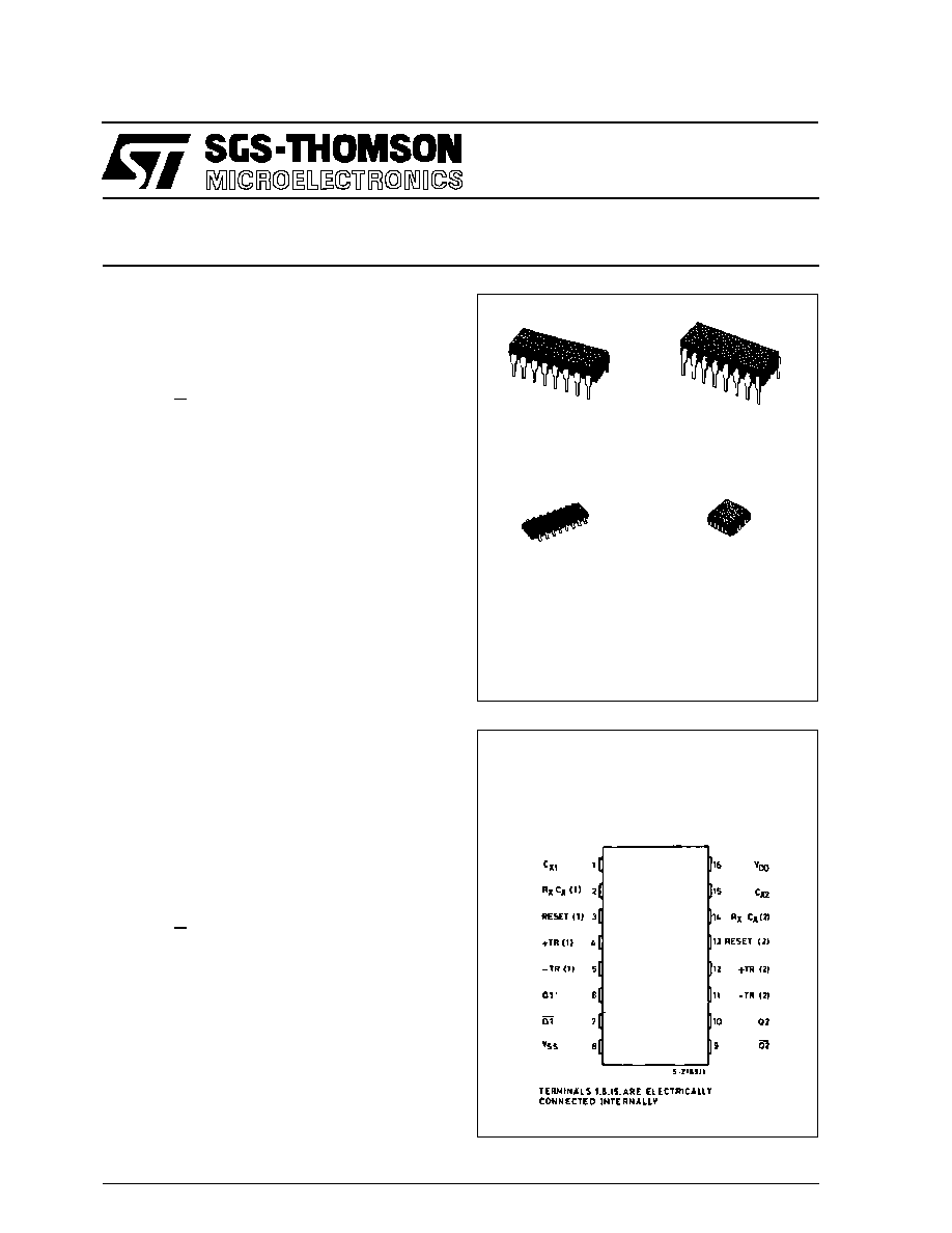
EY
(Plastic Package)
DESCRIPTION
ORDER CODES :
HCC4538BF
HCF4538BM1
HCF4538BEY
HCF4538BC1
F
(Ceramic Package)
M1
(Micro Package)
C1
(Chip Carrier)
PIN CONNECTIONS
The HCC4538B (extended temperature range) and
HCF4538B (intermediate temperature range) are
monolithic integrated circuit, available in 16-lead
dual in-line plastic or-ceramic package and plastic
micro package. The HCC/HCF4538B dual precision
monostable multivibrator provides stable retrigger-
able/resettable one-shot operation for any fixed-
voltage timing application. An external resistor (R
X
)
and an external capacitor (C
X
) control the timing and
accuracy for the circuit. Adjustment of R
X
and C
X
provides a wide range of output pulse widths from
the Q and Q terminals. The time delay from trigger
input to output transition (trigger propagation delay)
and the time delay from reset input to output transi-
tion (reset propagation delay) are independent of R
X
and C
X
. Precision control of output pulse widths is
achieved through linear CMOS techniques. Lead-
ing-edge-triggering (+ TR) and trailing-edge-trigger-
ing (≠ TR) inputs are provided for triggering from
either edge of an input pulse. An unused + TR input
should be tied to V
SS
. An unused ≠ TR input should
be tied to V
DD
. A RESET (on low level) is provided
for immediate termination of the output pulse or to
.
RETRIGGERABLE/RESETTABLE
CAPABILITY
.
TRIGGER AND RESET PROPAGATION DE-
LAYS INDEPENDENT OF R
X
, C
X
.
TRIGGERING FROM LEADING OR TRAILING
EDGE
.
Q AND Q BUFFERED OUTPUTS AVAILABLE
.
SEPARATE RESETS
.
WIDE RANGE OF OUTPUT-PULSE WIDTHS
.
QUIESCENT CURRENT SPECIFIED TO 20V
FOR HCC DEVICE
.
5V, 10V, AND 15V PARAMETRIC RATINGS
.
SCHMITT TRIGGER INPUT ALLOWS UN-
LIMITER RISE AND FALL TIMES ON + TR AND
≠ TR INPUTS
.
INPUT CURRENT OF 100nA AT 18V AND 25
∞
C
FOR HCC DEVICE
.
100% TESTED FOR QUIESCENT CURRENT
.
MEETS ALL REQUIREMENTS OF JEDEC TEN-
TATIVE STANDARD N
∞
13A, "STANDARD SPE-
CIFICATIONS FOR DESCRIPTION OF "B"
SERIES CMOS DEVICES"
1/14
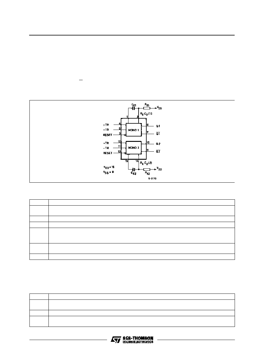
FUNCTIONAL DIAGRAM
ABSOLUTE MAXIMUM RATING
Symbol
Parameter
Value
Unit
V
DD
*
Supply Voltage: HCC Types
HCF Types
-0.5 to +20
-0.5 to +18
V
V
V
i
Input Voltage
-0.5 to V
DD
+ 0.5
V
I
I
DC Input Current (any one input)
±
10
mA
P
tot
Total Power Dissipation (per package)
Dissipation per Output Transistor
for Top = Full Package Temperature Range
200
100
mW
mW
T
op
Operating Temperature: HCC Types
HCF Types
-55 to +125
-40 to +85
o
C
o
C
T
stg
Storage Temperature
-65 to +150
o
C
Stresses above those listed under "Absolute Maximum Ratings" may cause permanent damage to the device. This is a stress ratingonly and functional
operation of the device at these or any other conditions above those indicated in the operational sections of this specification is not implied. Exposure
to absolute maximum rating conditions for external periods may affect device reliability.
* All voltage values are referred to V
SS
pin voltage.
RECOMMENDED OPERATING CONDITIONS
Symbol
Parameter
Value
Unit
V
DD
Supply Voltage: HCC Types
HCF Types
3 to 18
3 to 15
V
V
V
I
Input Voltage
0 to V
DD
V
T
op
Operating Temperature: HCC Types
HCF Types
-55 to +125
-40 to +85
o
C
o
C
prevent output pulses when power is turned on. An
unused RESET input should be tied to V
DD
. How-
ever, if an entire section of the HCC/HCF4538B is
not used, its inputs must be tied to either V
DD
or V
SS
(see table 1). In normal operation the circuit triggers
(extends the output pulse one period) on the appli-
cation of each new trigger pulse. For operation in the
non-retriggerable mode, Q is connected to ≠ TR
when leading-edge triggering (+ TR) is used or Q is
connected to + TR when trailingedge triggering (≠
TR) is used. The time period (T) for this multivibrator
can be calculated by : T = R
X
C
X
. The min. value of
external resistance, R
X
, is 4K
. The max. and min.
values of external capacitance, C
X
, are 100
µ
F and
5nF, respectively.
HCC/HCF4538B
2/14
Notes : 1. A Retriggerable one-shot multivibrator has an output pulse width which is extended on full time period (T) after application of the last
trigger pulse.
2. A Non-retriggerable one-shot multivibrator has a time period (T) referenced from the application of the first trigger pulse.
LOGIC DIAGRAM (1/2 of device shown)
TABLE 1: Functional Terminal Connections
Function
V
DD
to Term. NO
V
SS
to Term. NO
Input Pulse to
Term. No
Other
Connections
Mono
(1)
Mono
(2)
Mono
(1)
Mono
(2)
Mono
(1)
Mono
(2)
Mono
(1)
Mono
(2)
Leading-Edge
Trigger/Retriggerable
3, 5
11, 13
4
12
Leading-Edge
Trigger/Non-retriggerable
3
13
4
12
5, 7
11, 9
Trailing-Edge
Trigger/Retriggerable
3
13
4
12
5
11
Trailing-Edge
Trigger/Non-retriggerable
3
13
5
11
4, 6
12, 10
Pulse Width
HCC/HCF4538B
3/14

STATIC ELECTRICAL CHARACTERISTICS (over recommended operating conditions)
Symbol
Parameter
Test Conditios
Value
Unit
V
I
(V)
V
O
(V)
|I
O
|
(
µ
A)
V
DD
(V)
T
LOW
*
25
o
C
T
HIGH
*
Min.
Max.
Min.
Typ.
Max.
Min.
Max.
I
L
Quiescent
Current
HCC
Types
0/5
5
5
0.04
5
150
µ
A
0/10
10
10
0.04
10
300
0/15
15
20
0.04
20
600
0/20
20
100
0.08
100
3000
HCF
Types
0/5
5
5
0.04
5
150
0/10
10
10
0.04
10
300
0/15
15
20
0.04
20
600
V
OH
Output High
Voltage
0/5
< 1
5
4.95
4.95
5
4.95
V
0/10
< 1
10
9.95
9.95
10
9.95
0/15
< 1
15
14.95
14.95
15
14.95
V
OL
Output Low
Voltage
5/0
< 1
5
0.05
0.05
0.05
V
10/0
< 1
10
0.05
0.05
0.05
15/0
< 1
15
0.05
0.05
0.05
V
IH
Input High
Voltage
0.5/4.5
< 1
5
3.5
3.5
3.5
V
1/9
< 1
10
7
7
7
1.5/13.5
< 1
15
11
11
11
V
IL
Input Low
Voltage
4.5/0.5
< 1
5
1.5
1.5
1.5
V
9/1
< 1
10
3
3
3
13.5/1.5
< 1
15
4
4
4
I
OH
Output
Drive
Current
HCC
Types
0/5
2.5
5
-2
-1.6
-3.2
-1.15
mA
0/5
4.6
5
-0.64
-0.51
-1
-0.36
0/10
9.5
10
-1.6
-1.3
-2.6
-0.9
0/15
13.5
15
-4.2
-3.4
-6.8
-2.4
HCF
Types
0/5
2.5
5
-1.8
-1.6
-3.2
-1.3
0/5
4.6
5
-0.61
-0.51
-1
-0.42
0/10
9.5
10
-1.5
-1.3
-2.6
-1.1
0/15
13.5
15
-4
-3.4
-6.8
-2.8
I
OL
Output
Sink
Current
HCC
Types
0/5
0.4
5
0.64
0.51
1
0.36
mA
0/10
0.5
10
1.6
1.3
2.6
0.9
0/15
1.5
15
4.2
3.4
6.8
2.4
HCF
Types
0/5
0.4
5
0.61
0.51
1
0.42
0/10
0.5
10
1.5
1.3
2.6
1.1
0/15
1.5
15
3.6
3.4
6.8
2.8
I
IH
, I
IL
Input Leakage
Current
0/18
Any Input
18
±
0.1
±
10
-5
±
0.1
±
1
µ
A
C
I
Input Capacitance
Any Input
5
7.5
pF
* T
LOW
= -55
o
C for HCC device: -40
o
C for HCF device.
* T
HIGH
= +125
o
C for HCC device: +85
o
C for HCF device.
The Noise Margin for both "1" and "0" level is: 1V min. with V
DD
= 5 V, 2 V min. with V
DD
= 10 V, 2.5 V min. with V
DD
= 15 V
HCC/HCF4538B
4/14
DYNAMIC ELECTRICAL CHARACTERISTICS (T
amb
= 25
o
C, C
L
= 50 pF, R
L
= 200 K
,
typical temperature coefficent for all V
DD
values is 03 %/
o
C, all input rise and fall times= 20 ns)
Symbol
Parameter
Test Conditions
Value
Unit
V
DD
(V)
Min.
Typ.
Max.
t
TLH
t
THL
Transition Time
5
100
200
ns
10
50
100
15
40
80
t
PLH
t
PHL
Propagation Delay Time
+TR or -TR to Q or Q
5
300
600
ns
10
150
300
15
100
220
t
PLH
t
PHL
Propagation Delay Time
Reset to Q or Q
R
L
= 1K
5
250
500
ns
10
125
250
15
95
190
t
WH
t
WL
Minimum Input Pulse Width
+TR, -TR or Reset
R
L
= 1K
5
80
140
ns
10
40
80
15
30
60
t
WT
Output Pulse Width - Q or Q
(C
X
= 0.005
µ
F, R
X
= 10 K
*)
5
57
60.6
64.5
µ
s
10
55
58.9
63.0
15
55
59.1
63.5
t
WT
Output Pulse Width - Q or Q
(C
X
= 0.1
µ
F, R
X
= 100 K
)
5
9.4
9.97
10.5
ms
10
9.4
9.95
10.6
15
9.5
10.00
10.6
t
WT
Output Pulse Width - Q or Q
(C
X
= 10
µ
F, R
X
= 100 K
)
5
0.95
1.00
1.06
s
10
0.95
1.00
1.06
15
0.96
1.00
1.07
t
W
Pulse Width Match Between
Circuits in Same Package:
100
(
T
1
-
T
2
)
T
1
(C
X
= 0.1
µ
F, R
X
= 100 K
)
5
±
1
%
10
±
1
15
±
1
t
rr
Minimum Retrigger Time
5
0
ns
10
0
15
0
C
IN
Input Capacitance
Any
Input
5
7.5
pF
* Minimum R
X
value = 4 K
, minimum C
X
value = 500 pF
HCC/HCF4538B
5/14