 | –≠–ª–µ–∫—Ç—Ä–æ–Ω–Ω—ã–π –∫–æ–º–ø–æ–Ω–µ–Ω—Ç: HD1520FX | –°–∫–∞—á–∞—Ç—å:  PDF PDF  ZIP ZIP |

1/8
May 2005
n
STATE-OF-THE-ART TECHNOLOGY:
DIFFUSED COLLECTOR "ENHANCED
GENERATION" EHVS1
n
WIDER RANGE OF OPTIMUM DRIVE
CONDITIONS
n
LESS SENSITIVE TO OPERATING
TEMPERATURE VARIATION
n
FULLY INSULATED POWER PACKAGE U.L.
COMPLIANT
APPLICATIONS
n
HORIZONTAL DEFLECTION FOR LARGE
AND FLAT SCREEN 100 Hz COLOR TVs
DESCRIPTION
The device is manufactured using Diffused
Collector in Planar technology adopting "Enhance
High Voltage Structure" (EHVS1) developed to fit
High-Definition CRT displays.
The new HD product series show improved silicon
efficiency bringing updated performance to the
Horizontal Deflection stage.
Figure 1: Package
Figure 2: Internal Schematic Diagram
Table 1:
Table 2: Absolute Maximum Ratings
ISOWATT218FX
Part Number
Marking
Package
Packaging
HD1520FX
HD1520FX
ISOWATT218FX
TUBE
Symbol
Parameter
Value
Unit
V
CES
Collector-Emitter Voltage (V
BE
= 0)
1500
V
V
CEO
Collector-Emitter Voltage (I
B
= 0)
700
V
V
EBO
Emitter-Base Voltage (I
C
= 0)
10
V
I
C
Collector Current
15
A
I
CM
Collector Peak Current (t
p
< 5ms)
22
A
I
B
Base Current
8
A
I
BM
Base Peak Current (t
p
< 5ms)
12
A
P
tot
Total Dissipation at T
C
= 25
o
C
64
W
V
ins
Insulation Withstand Voltage (RMS) from All Three Leads to
External Heatsink
2500
V
HD1520FX
HIGH VOLTAGE NPN POWER TRANSISTOR
FOR HIGH DEFINITION CRT DISPLAYS
Rev. 1
HD1520FX
2/8
Table 3: Thermal Data
Table 4: Electrical Characteristics (T
case
= 25
o
C unless otherwise specified)
* Pulsed: Pulsed duration = 300 ms, duty cycle
1.5
%.
T
stg
Storage Temperature
-65 to 150
∞C
T
J
Max. Operating Junction Temperature
150
∞C
R
thj-case
Thermal Resistance Junction-Case Max
1.95
o
C/W
Symbol
Parameter
Test Conditions
Min.
Typ.
Max.
Unit
I
CES
Collector Cut-off Current
(V
BE
= 0)
V
CE
= 1500 V
V
CE
= 1500 V T
C
= 125
o
C
0.2
2
mA
mA
I
EBO
Emitter Cut-off Current
(I
C
= 0)
V
EB
= 5 V
10
µA
V
CEO(sus)
* Collector-Emitter
Sustaining Voltage
(I
B
= 0 )
I
C
= 100 mA
700
V
V
EBO
Emitter-Base Voltage
(I
C
= 0 )
I
E
= 10 mA
10
V
V
CE(sat)
*
Collector-Emitter
Saturation Voltage
I
C
= 9 A I
B
= 1.8 A
3
V
V
BE(sat)
*
Base-Emitter Saturation
Voltage
I
C
= 9 A I
B
= 1.8 A
1.3
V
h
FE
DC Current Gain
I
C
= 1 A V
CE
= 5 V
I
C
= 9 A V
CE
= 1 V
I
C
= 9 A V
CE
= 5 V
5.5
26
5
9.5
t
s
t
f
INDUCTIVE LOAD
Storage Time
Fall Time
I
C
= 9 A f
h
= 31250 Hz
I
B(on)
= 1.3 A I
B(off)
= -4.2 A
L
BB(on)
= 1.9 µH V
BE(off)
= -2.7 V
V
CE(fly)
= 1040 V
3.2
220
4
300
µs
ns
Symbol
Parameter
Value
Unit
HD1520FX
3/8
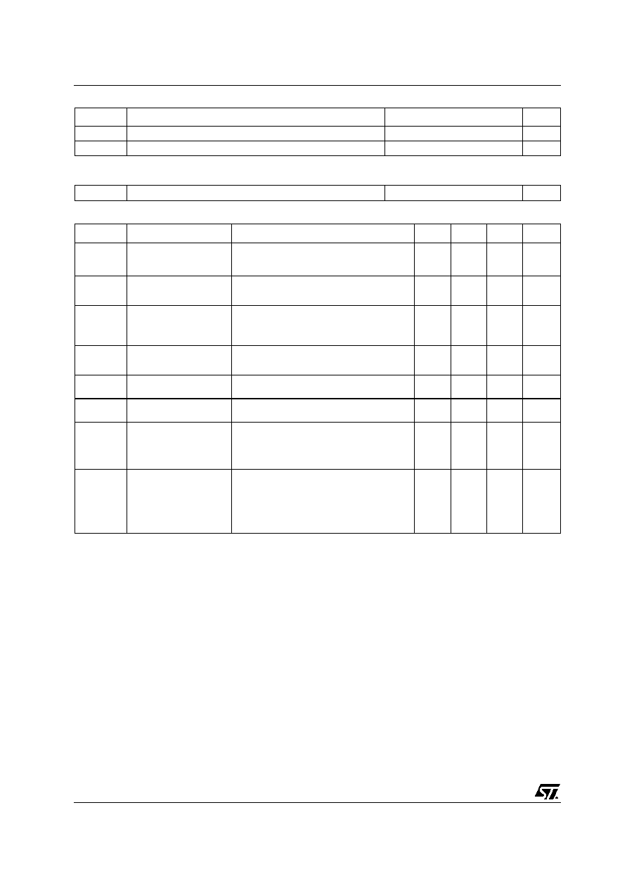
Figure 3: Safe Operating Area
Figure 4: Output Chatacterisctics
Figure 5: DC Current Gain
Figure 6: Derating Curve
Figure 7: Reverse Biased SOA
Figure 8: DC Current Gain
HD1520FX
4/8
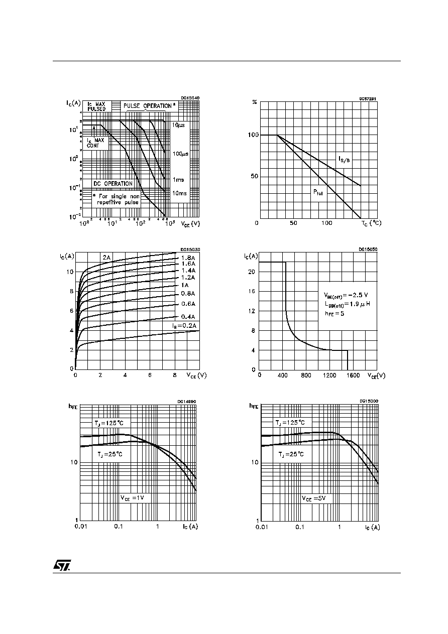
Figure 9: Collector-Emitter Saturation Voltage
Figure 10: Power Losses
Figure 11: Base-Emitter Saturation Voltage
Figure 12: Inductive Load Switching Time
HD1520FX
5/8
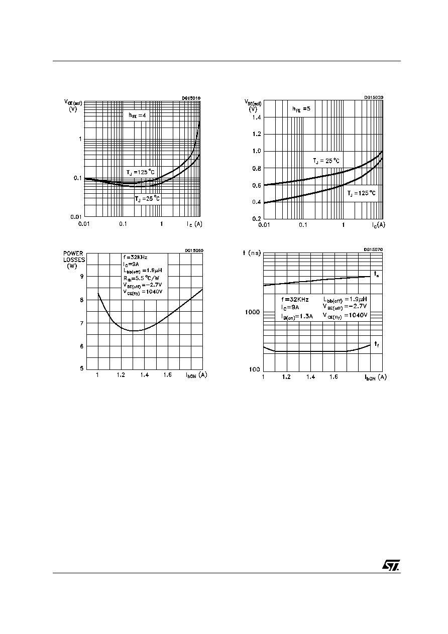
Figure 13: Power Losses and Inductive Load Switching Test Circuit
Figure 14: Reverse Biased Safe Operating Area Test Circuit