 | –≠–ª–µ–∫—Ç—Ä–æ–Ω–Ω—ã–π –∫–æ–º–ø–æ–Ω–µ–Ω—Ç: HD1760JL | –°–∫–∞—á–∞—Ç—å:  PDF PDF  ZIP ZIP |
November 2005
1/8
8
HD1760JL
High Voltage NPN Power Transistor
for High Definition and New Super-Slim CRT Display
Features
STATE-OF-THE-ART TECHNOLOGY:
DIFFUSED COLLECTOR "ENHANCED
GENERATION" EHVS1
WIDER RANGE OF OPTIMUM DRIVE
CONDITIONS
LESS SENSITIVE TO OPERATING
TEMPERATURE VARIATION
Applications
HORIZONTAL DEFLECTION OUTPUT FOR
DIGITAL TV, HDTV AND HIGH -END
MONITORS
Description
The device uses a Diffused Collector in Planar
technology which adopts "Enhanced High Voltage
Structure" (EHVS1) that was developed to fit
High-Definition CRT displays.
The new HD product series features improved
silicon efficiency, bringing updated performance to
Horizontal Deflection output stages.
Order codes
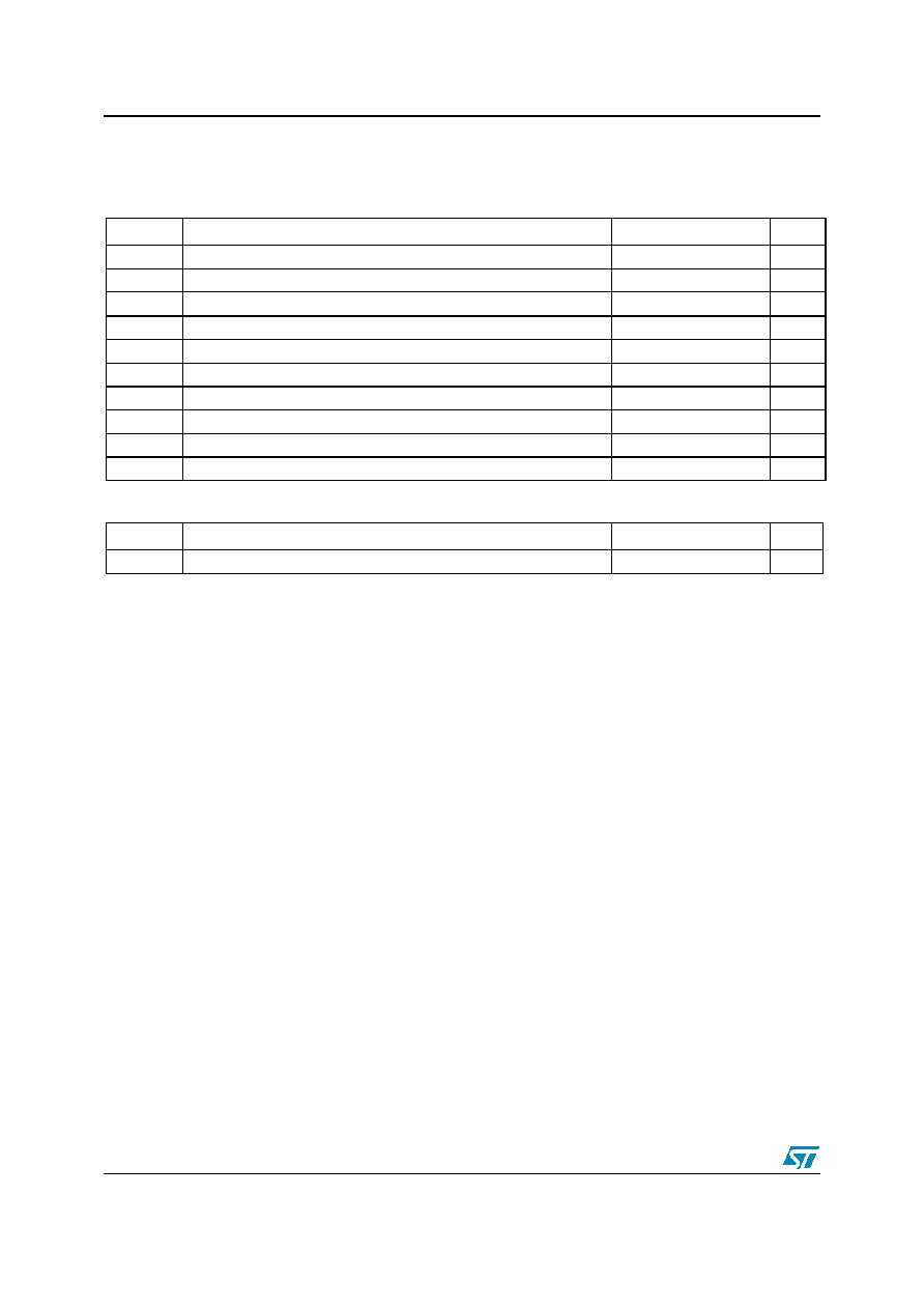
Internal Schematic Diagram
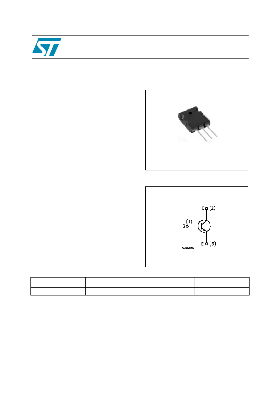
TO-264
1
2
3
www.st.com
PRELIMINARY DATA
Part Number
Marking
Package
Packing
HD1760JL
HD1760JL
TO-264
TUBE
rev.2
1 Electrical ratings
HD1760JL
2/8
1 Electrical
ratings
Table 1.
Absolute Maximum Rating
Table 2.
Thermal Data
Symbol
Parameter
Value
Unit
V
CES
Collector-Emitter Voltage (V
BE
= 0)
1700
V
V
CEO
Collector-Emitter Voltage (I
B
= 0)
800
V
V
EBO
Emitte-Base Voltage (I
C
= 0)
10
V
I
C
Collector Current
36
A
I
CM
Collector Peak Current (t
P
< 5ms)
54
A
I
B
Base Current
18
A
I
BM
Base Peak Current (t
P
< 5ms)
27
A
P
TOT
Total dissipation at T
c
= 25∞C
200
W
T
STG
Storage Temperature
-65 to 150
∞C
T
J
Max. Operating Junction Temperature
150
∞C
Symbol
Parameter
Value
Unit
R
thJC
Thermal Resistance Junction-Case
____________________
Max
0.625
∞C/W
HD1760JL
2 Electrical Characteristics
3/8
2 Electrical
Characteristics
(T
CASE
= 25∞C; unless otherwise specified)
Table 3.
Electrical Characteristics
Note: 1 Pulsed duration = 300
s, duty cycle
1.5%.
Symbol
Parameter
Test Conditions
Min.
Typ.
Max.
Unit
I
CES
Collector Cut-off Current
(V
BE
= 0)
V
CE
= 1700V
V
CE
= 1700V
___ _
T
C
= 125∞C
0.2
2
mA
mA
I
EBO
Emitter Cut-off Current
(I
C
= 0)
V
EB
= 5V
10
A
V
CEO(sus)
Note: 1
Collector-Emitter
Sustaining Voltage (I
B
= 0)
I
C
= 10mA
800
V
V
EBO
Emitter-Base Voltage (I
C
= 0)
I
E
= 10mA
10
V
V
CE(sat)
Note: 1
Collector-Emitter Saturation
Voltage
I
C
= 18A
_____
I
B
= 4.5A
2
V
V
BE(sat)
Note: 1
Base-Emitter Saturation Voltage
I
C
= 18A
_____
I
B
= 4.5A
1.5
V
h
FE
DC Current Gain
I
C
= 2A
_____
V
CE
= 5V
I
C
= 18A
____
V
CE
= 5V
5
30
8.5
t
s
t
f
INDUCTIVE LOAD
Storage Time
Fall Time
I
C
= 12A
____ _ __
f
h
= 32 KHz
I
B(on)
= 1A
___ _ _
I
B(off)
= -6.9A
V
CE(fly)
= 1340V
__
V
BE(off)
= -2.7V
L
BB(on)
= 0.8
H
2.6
300
s
ns
t
s
t
f
INDUCTIVE LOAD
Storage Time
Fall Time
I
C
= 8A
____ _ __
f
h
= 100kHz
I
B(on)
= 1.3A
___ _ _
I
B(off)
= -5.8A
V
CE(fly)
= 1300V
__
V
BE(off)
= -2.7V
L
BB(on)
= 0.25
H
2
110
s
ns
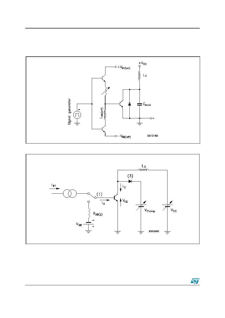
3 Test circuit
HD1760JL
4/8
3 Test
circuit
Figure 1.
Power Losses and Inductive Load Switching Test Circuit
Figure 2.
Reverse Biased Safe Operating Area Test Circuit
HD1760JL
4 Package Mechanical Data
5/8
4
Package Mechanical Data
In order to meet environmental requirements, ST offers these devices in ECOPACKÆ
packages. These packages have a Lead-free second level interconnect . The category of
second level interconnect is marked on the package and on the inner box label, in compliance
with JEDEC Standard JESD97. The maximum ratings related to soldering conditions are also
marked on the inner box label. ECOPACK is an ST trademark. ECOPACK specifications are
available at: www.st.com