 | ÐлекÑÑоннÑй компоненÑ: IRF620FP | СкаÑаÑÑ:  PDF PDF  ZIP ZIP |
OLD PRODUCT:NOT SUITABLE FOR NEW DESIGN-IN
1/9
August 2000
IRF620
IRF620FP
N-CHANNEL 200V - 0.6
- 6A TO-220/FP
PowerMeshTMII MOSFET
(1)I
SD
6A, di/dt
300A/µs, V
DD
V
(BR)DSS
, T
j
T
JMAX.
(**) Limited only by Maximum Temperature Allowed
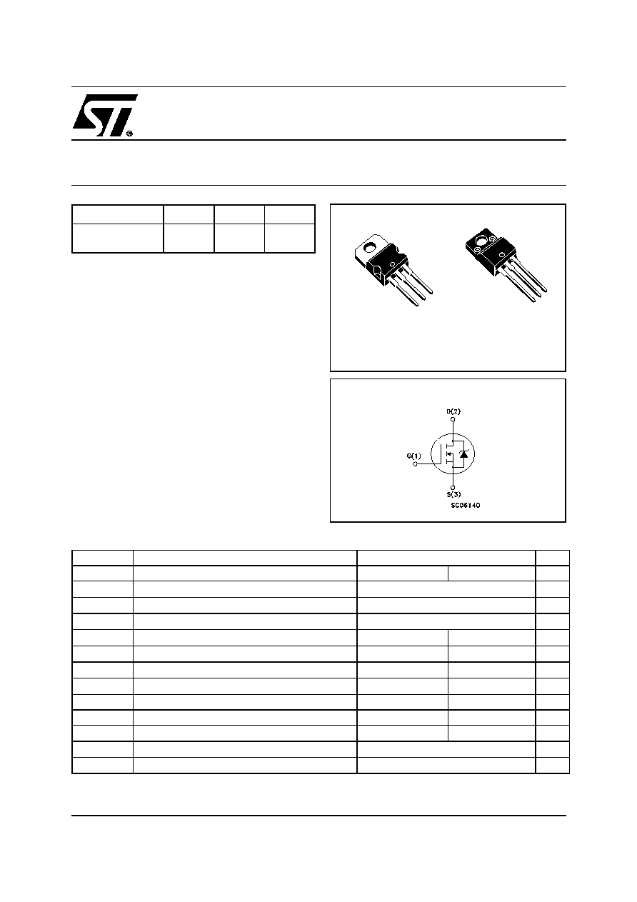
INTERNAL SCHEMATIC DIAGRAM
s
TYPICAL R
DS
(on) = 0.6
s
EXTREMELY HIGH dv/dt CAPABILITY
s
100% AVALANCHE TESTED
s
NEW HIGH VOLTAGE BENCHMARK
s
GATE CHARGE MINIMIZED
DESCRIPTION
The PowerMESH
TM
II is
the evolution of the first
generation of MESH OVERLAY
TM.
The layout re-
finements introduced greatly improve the Ron*area
figure of merit while keeping the device at the lead-
ing edge for what concerns switching speed, gate
charge and ruggedness.
APPLICATIONS
s
HIGH CURRENT, HIGH SPEED SWITCHING
s
SWITH MODE POWER SUPPLIES (SMPS)
s
DC-AC CONVERTERS FOR WELDING
EQUIPMENT AND UNINTERRUPTIBLE
POWER SUPPLIES AND MOTOR DRIVES
ABSOLUTE MAXIMUM RATINGS
(·)Pulse width limited by safe operating area
TYPE
V
DSS
R
DS(on)
I
D
IRF620
IRF620FP
200 V
200 V
< 0.8
< 0.8
6 A
6 A
Symbol
Parameter
Value
Unit
IRF620
IRF620FP
V
DS
Drain-source Voltage (V
GS
= 0)
200
V
V
DGR
Drain-gate Voltage (R
GS
= 20 k
)
200
V
V
GS
Gate- source Voltage
±20
V
I
D
Drain Current (continuous) at T
C
= 25°C
6
6 (**)
A
I
D
Drain Current (continuous) at T
C
= 100°C
3.8
3.8 (**)
A
I
DM
(
l
)
Drain Current (pulsed)
24
24
A
P
TOT
Total Dissipation at T
C
= 25°C
70
30
W
Derating Factor
0.56
0.24
W/°C
dv/dt (1)
Peak Diode Recovery voltage slope
5
5
V/ns
V
ISO
Insulation Winthstand Voltage (DC)
--
2000
V
T
stg
Storage Temperature
65 to 150
°C
T
j
Max. Operating Junction Temperature
150
°C
1
2
3
TO-220
1
2
3
TO-220FP
IRF620 / FP
2/9
THERMAL DATA
AVALANCHE CHARACTERISTICS
ELECTRICAL CHARACTERISTICS (T
CASE
= 25 °C UNLESS OTHERWISE SPECIFIED)
OFF
ON
(1)
DYNAMIC
TO-220
TO-220FP
Rthj-case
Thermal Resistance Junction-case Max
1.79
4.17
°C/W
Rthj-amb
Thermal Resistance Junction-ambient Max
62.5
°C/W
Rthc-sink
Thermal Resistance Case-sink Typ
0.5
°C/W
T
l
Maximum Lead Temperature For Soldering Purpose
300
°C
Symbol
Parameter
Max Value
Unit
I
AR
Avalanche Current, Repetitive or Not-Repetitive
(pulse width limited by T
j
max)
6
A
E
AS
Single Pulse Avalanche Energy
(starting T
j
= 25 °C, I
D
= I
AR
, V
DD
= 50 V)
160
mJ
Symbol
Parameter
Test Conditions
Min.
Typ.
Max.
Unit
V
(BR)DSS
Drain-source
Breakdown Voltage
I
D
= 250 µA, V
GS
= 0
200
V
I
DSS
Zero Gate Voltage
Drain Current (V
GS
= 0)
V
DS
= Max Rating
1
µA
V
DS
= Max Rating, T
C
= 125 °C
50
µA
I
GSS
Gate-body Leakage
Current (V
DS
= 0)
V
GS
= ±20 V
±100
nA
Symbol
Parameter
Test Conditions
Min.
Typ.
Max.
Unit
V
GS(th)
Gate Threshold Voltage
V
DS
= V
GS
, I
D
= 250 µA
2
3
4
V
R
DS(on)
Static Drain-source On
Resistance
V
GS
= 10 V, I
D
= 3 A
0.6
0.8
I
D(on)
On State Drain Current
V
DS
> I
D(on)
x R
DS(on)max,
V
GS
= 10 V
6
A
Symbol
Parameter
Test Conditions
Min.
Typ.
Max.
Unit
g
fs
(1)
Forward Transconductance
V
DS
> I
D(on)
x R
DS(on)max,
I
D
= 3A
1.5
4
S
C
iss
Input Capacitance
V
DS
= 25 V, f = 1 MHz, V
GS
= 0
350
pF
C
oss
Output Capacitance
70
pF
C
rss
Reverse Transfer
Capacitance
35
pF
3/9
IRF620 / FP
ELECTRICAL CHARACTERISTICS (CONTINUED)
SWITCHING ON
SWITCHING OFF
SOURCE DRAIN DIODE
Note: 1. Pulsed: Pulse duration = 300 µs, duty cycle 1.5 %.
2. Pulse width limited by safe operating area.
Symbol
Parameter
Test Conditions
Min.
Typ.
Max.
Unit
t
d(on)
Turn-on Delay Time
V
DD
= 100 V, I
D
= 3 A
R
G
= 4.7
V
GS
= 10 V
(see test circuit, Figure 3)
18
ns
t
r
Rise Time
30
ns
Q
g
Total Gate Charge
V
DD
= 160 V, I
D
= 6 A,
V
GS
= 10 V
19
27
nC
Q
gs
Gate-Source Charge
4.5
nC
Q
gd
Gate-Drain Charge
7.5
nC
Symbol
Parameter
Test Conditions
Min.
Typ.
Max.
Unit
t
r(Voff)
Off-voltage Rise Time
V
DD
= 160 V, I
D
= 6 A,
R
G
= 4.7
,
V
GS
= 10 V
(see test circuit, Figure 5)
40
ns
t
f
Fall Time
10
ns
t
c
Cross-over Time
65
ns
Symbol
Parameter
Test Conditions
Min.
Typ.
Max.
Unit
I
SD
Source-drain Current
6
A
I
SDM
(2)
Source-drain Current (pulsed)
24
A
V
SD
(1)
Forward On Voltage
I
SD
= 6 A, V
GS
= 0
1.5
V
t
rr
Reverse Recovery Time
I
SD
=6 A, di/dt = 100 A/µs
V
DD
= 100 V, T
j
= 150°C
(see test circuit, Figure 5)
155
ns
Q
rr
Reverse Recovery Charge
700
nC
I
RRM
Reverse Recovery Current
9
A
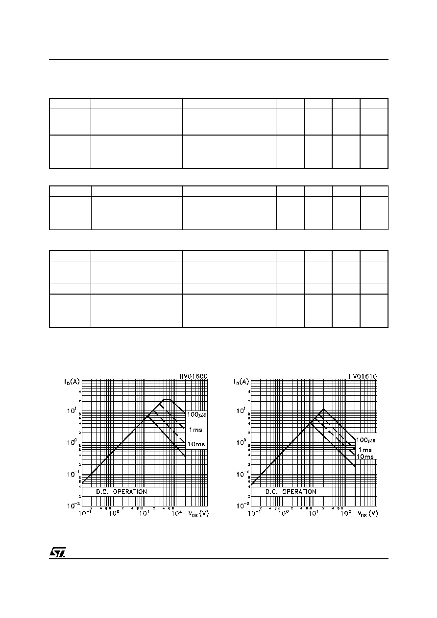
Safe Operating Area for TO-220
Safe Operating Area for TO-220FP
IRF620 / FP
4/9
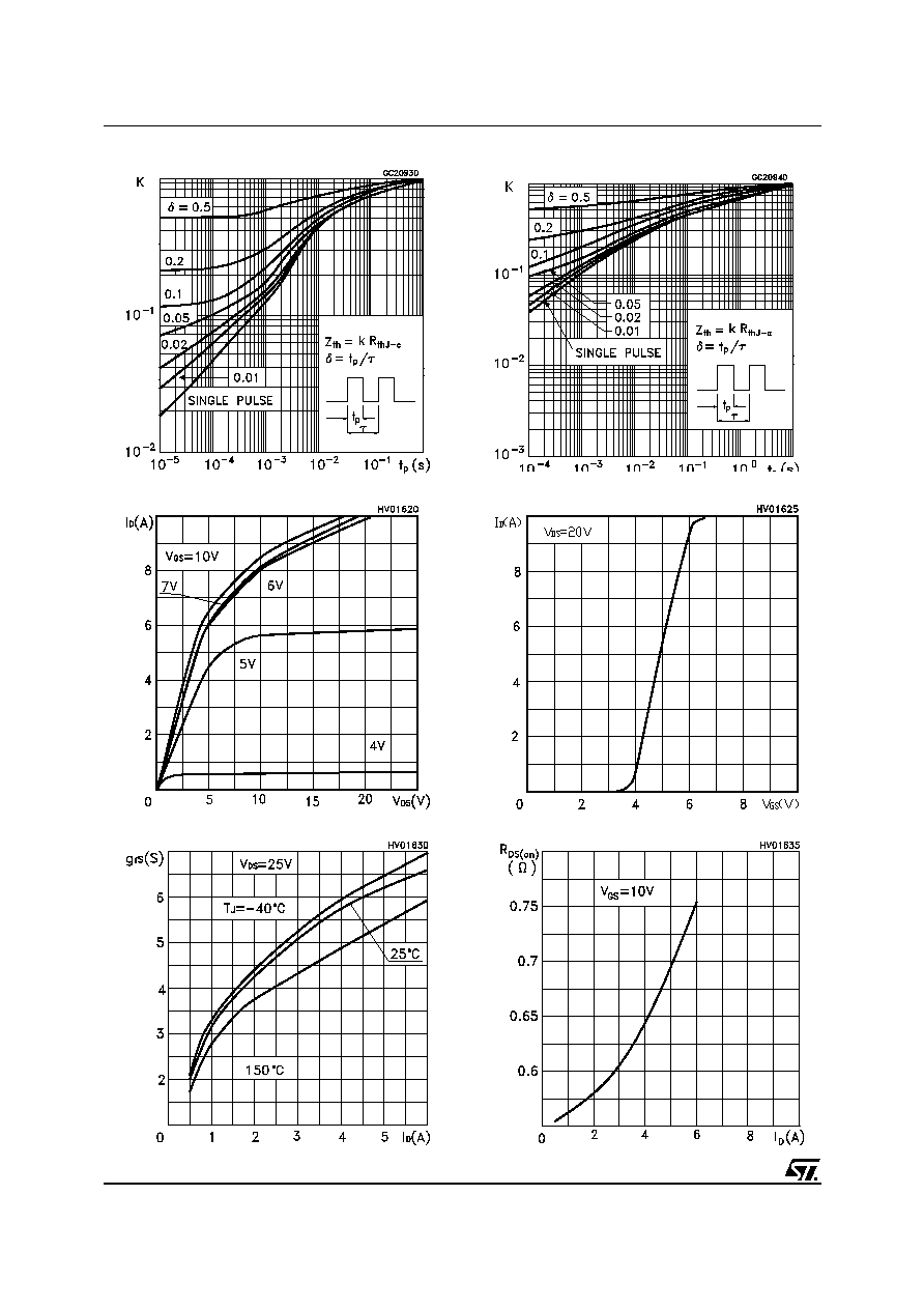
Transconductance
Transfer Characteristics
Output Characteristics
Thermal Impedence for TO-220
Static Drain-source On Resistance
Thermal Impedence for TO-220FP
5/9
IRF620 / FP
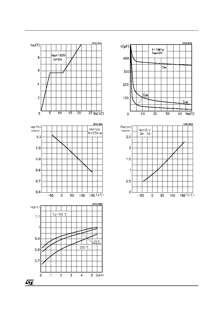
Capacitance Variations
Normalized On Resistance vs Temperature
Source-drain Diode Forward Characteristics
Normalized Gate Threshold Voltage vs Temp.
Gate Charge vs Gate-source Voltage
IRF620 / FP
6/9
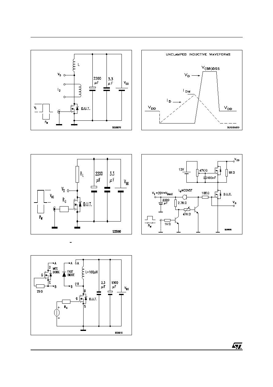
Fig. 5: Test Circuit For Inductive Load Switching
And Diode Recovery Times
Fig. 4: Gate Charge test Circuit
Fig. 2: Unclamped Inductive Waveform
Fig. 1: Unclamped Inductive Load Test Circuit
Fig. 3: Switching Times Test Circuit For
Resistive Load
7/9
IRF620 / FP
DIM.
mm
inch
MIN.
TYP.
MAX.
MIN.
TYP.
MAX.
A
4.40
4.60
0.173
0.181
C
1.23
1.32
0.048
0.051
D
2.40
2.72
0.094
0.107
D1
1.27
0.050
E
0.49
0.70
0.019
0.027
F
0.61
0.88
0.024
0.034
F1
1.14
1.70
0.044
0.067
F2
1.14
1.70
0.044
0.067
G
4.95
5.15
0.194
0.203
G1
2.4
2.7
0.094
0.106
H2
10.0
10.40
0.393
0.409
L2
16.4
0.645
L4
13.0
14.0
0.511
0.551
L5
2.65
2.95
0.104
0.116
L6
15.25
15.75
0.600
0.620
L7
6.2
6.6
0.244
0.260
L9
3.5
3.93
0.137
0.154
DIA.
3.75
3.85
0.147
0.151
L6
A
C
D
E
D1
F
G
L7
L2
Dia.
F1
L5
L4
H2
L9
F2
G1
TO-220 MECHANICAL DATA
P011C
IRF620 / FP
8/9
L2
A
B
D
E
H
G
L6
F
L3
G1
1 2 3
F2
F1
L7
L4
L5
DIM.
mm.
inch
MIN.
TYP
MAX.
MIN.
TYP.
MAX.
A
4.4
4.6
0.173
0.181
B
2.5
2.7
0.098
0.106
D
2.5
2.75
0.098
0.108
E
0.45
0.7
0.017
0.027
F
0.75
1
0.030
0.039
F1
1.15
1.7
0.045
0.067
F2
1.15
1.7
0.045
0.067
G
4.95
5.2
0.195
0.204
G1
2.4
2.7
0.094
0.106
H
10
10.4
0.393
0.409
L2
16
0.630
L3
28.6
30.6
1.126
1.204
L4
9.8
10.6
.0385
0.417
L5
2.9
3.6
0.114
0.141
L6
15.9
16.4
0.626
0.645
L7
9
9.3
0.354
0.366
Ø
3
3.2
0.118
0.126
TO-220FP MECHANICAL DATA

9/9
IRF620 / FP
Information furnished is believed to be accurate and reliable. However, STMicroelectronics assumes no responsibility for the
consequences of use of such information nor for any infringement of patents or other rights of third parties which may result from
its use. No license is granted by implication or otherwise under any patent or patent rights of STMicroelectronics. Specifications
mentioned in this publication are subject to change without notice. This publication supersedes and replaces all information
previously supplied. STMicroelectronics products are not authorized for use as critical components in life support devices or
systems without express written approval of STMicroelectronics.
© The ST logo is a registered trademark of STMicroelectronics
© 2002 STMicroelectronics - Printed in Italy - All Rights Reserved
STMicroelectronics GROUP OF COMPANIES
Australia - Brazil - Canada - China - Finland - France - Germany - Hong Kong - India - Israel - Italy - Japan - Malaysia - Malta - Morocco
Singapore - Spain - Sweden - Switzerland - United Kingdom - United States.
© http://www.st.com