 | –≠–ª–µ–∫—Ç—Ä–æ–Ω–Ω—ã–π –∫–æ–º–ø–æ–Ω–µ–Ω—Ç: IRF630M | –°–∫–∞—á–∞—Ç—å:  PDF PDF  ZIP ZIP |
1/9
October 2001
IRF630M
IRF630MFP
N-CHANNEL 200V - 0.35
- 9A TO-220/TO-220FP
MESH OVERLAYTM MOSFET
s
TYPICAL R
DS
(on) = 0.35
s
EXTREMELY HIGH dv/dt CAPABILITY
s
VERY LOW INTRINSIC CAPACITANCES
s
GATE CHARGE MINIMIZED
DESCRIPTION
This power MOSFET is designed using the compa-
ny's consolidated strip layout-based MESH OVER-
LAYTM process. This technology matches and
improves the performances compared with standard
parts from various sources.
Isolated TO-220 option simplifies assembly and cuts
risk of accidental short circuit in crowded monitor
PCB's.
.APPLICATIONS
s
MONITOR DISPLAYS
s
GENERAL PURPOSE SWITCH
ABSOLUTE MAXIMUM RATINGS
(∑)Pulse width limited by safe operating area
TYPE
V
DSS
R
DS(on)
I
D
IRF630M
200 V
< 0.40
9 A
IRF630FPM
200 V
< 0.40
9 A
Symbol
Parameter
Value
Unit
IRF630M
IRF630MFP
V
DS
Drain-source Voltage (V
GS
= 0)
200
V
V
DGR
Drain-gate Voltage (R
GS
= 20 k
)
200
V
V
GS
Gate- source Voltage
± 20
V
I
D
Drain Current (continuos) at T
C
= 25∞C
9
9 (**)
A
I
D
Drain Current (continuos) at T
C
= 100∞C
5.7
5.7 (**)
A
I
DM
(
q
)
Drain Current (pulsed)
36
36
A
P
TOT
Total Dissipation at T
C
= 25∞C
75
30
W
Derating Factor
0.6
0.24
W/∞C
dv/dt (1)
Peak Diode Recovery voltage slope
5
5
V/ns
V
ISO
Insulation Winthstand Voltage (DC)
--
2500
V
T
stg
Storage Temperature
≠65 to 150
∞C
T
j
Max. Operating Junction Temperature
150
∞C
(1)I
SD
9A, di/dt
300A/µs, V
DD
V
(BR)DSS
, T
j
T
JMAX.
(**) Limited only by Maximum Temperature Allowed
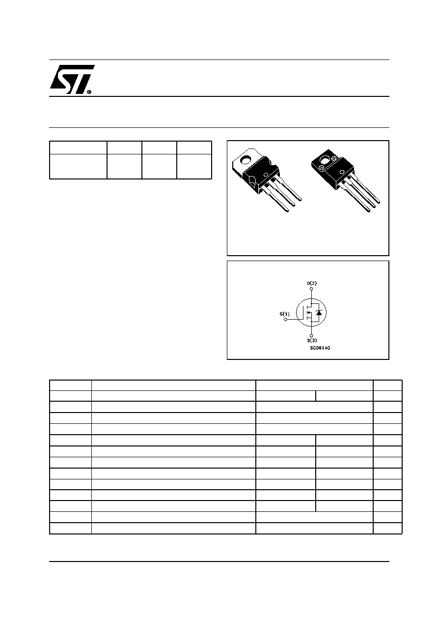
INTERNAL SCHEMATIC DIAGRAM
1
2
3
TO-220
1
2
3
TO-220FP
IRF630M / FP
2/9
THERMAL DATA
ELECTRICAL CHARACTERISTICS (TCASE = 25 ∞C UNLESS OTHERWISE SPECIFIED)
OFF
ON
(1)
DYNAMIC
TO-220
TO-220FP
Rthj-case
Thermal Resistance Junction-case Max
1.67
4.17
∞C/W
Rthj-amb
Thermal Resistance Junction-ambient Max
62.5
∞C/W
T
l
Maximum Lead Temperature For Soldering Purpose
300
∞C
Symbol
Parameter
Test Conditions
Min.
Typ.
Max.
Unit
V
(BR)DSS
Drain-source
Breakdown Voltage
I
D
= 250 µA, V
GS
= 0
200
V
I
DSS
Zero Gate Voltage
Drain Current (V
GS
= 0)
V
DS
= Max Rating
1
µA
V
DS
= Max Rating, T
C
= 125 ∞C
50
µA
I
GSS
Gate-body Leakage
Current (V
DS
= 0)
V
GS
= ± 20V
±100
nA
Symbol
Parameter
Test Conditions
Min.
Typ.
Max.
Unit
V
GS(th)
Gate Threshold Voltage
V
DS
= V
GS
, I
D
= 250µA
2
3
4
V
R
DS(on)
Static Drain-source On
Resistance
V
GS
= 10V, I
D
= 4.5 A
0.35
0.40
Symbol
Parameter
Test Conditions
Min.
Typ.
Max.
Unit
g
fs
(1)
Forward Transconductance
V
DS
> I
D(on)
x R
DS(on)max,
I
D
= 4.5 A
3
4
S
C
iss
Input Capacitance
V
DS
= 25V, f = 1 MHz, V
GS
= 0
540
700
pF
C
oss
Output Capacitance
90
120
pF
C
rss
Reverse Transfer
Capacitance
35
50
pF
3/9
IRF630M / FP
ELECTRICAL CHARACTERISTICS (CONTINUED)
SWITCHING ON
SWITCHING OFF
SOURCE DRAIN DIODE
Note: 1. Pulsed: Pulse duration = 300 µs, duty cycle 1.5 %.
2. Pulse width limited by safe operating area.
Symbol
Parameter
Test Conditions
Min.
Typ.
Max.
Unit
t
d(on)
Turn-on Delay Time
V
DD
= 100 V, I
D
= 4.5 A
R
G
= 4.7
V
GS
= 10 V
(see test circuit, Figure 3)
10
14
ns
t
r
Rise Time
15
20
ns
Q
g
Total Gate Charge
V
DD
= 160V, I
D
= 9 A,
V
GS
= 10V
31
45
nC
Q
gs
Gate-Source Charge
7.5
nC
Q
gd
Gate-Drain Charge
9
nC
Symbol
Parameter
Test Conditions
Min.
Typ.
Max.
Unit
t
r(Voff)
Off-voltage Rise Time
V
DD
= 160V, I
D
= 9 A,
R
G
= 4.7
,
V
GS
= 10V
(see test circuit, Figure 5)
12
17
ns
t
f
Fall Time
12
17
ns
t
c
Cross-over Time
25
35
ns
Symbol
Parameter
Test Conditions
Min.
Typ.
Max.
Unit
I
SD
Source-drain Current
9
A
I
SDM
(2)
Source-drain Current (pulsed)
36
A
V
SD
(1)
Forward On Voltage
I
SD
= 9 A, V
GS
= 0
1.5
V
t
rr
Reverse Recovery Time
I
SD
= 9 A, di/dt = 100A/µs
V
DD
= 50 V, T
j
= 150∞C
(see test circuit, Figure 5)
170
ns
Q
rr
Reverse Recovery Charge
0.95
µ
C
I
RRM
Reverse Recovery Current
11
A
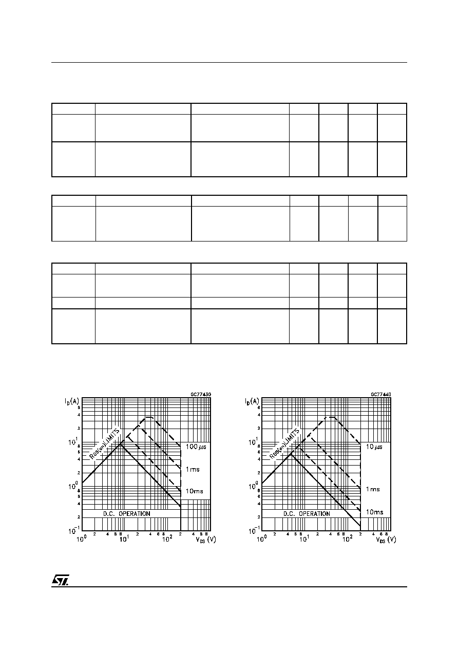
Safe Operating Area for TO-220FP
Safe Operating Area for TO-220
IRF630M / FP
4/9
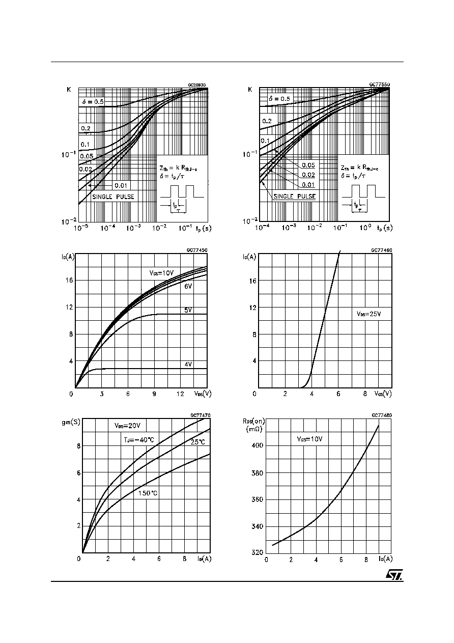
Static Drain-source On Resistance
Transconductance
Transfer Characteristics
Output Characteristics
Thermal Impedence for TO-220
Thermal Impedence for TO-220FP
5/9
IRF630M / FP
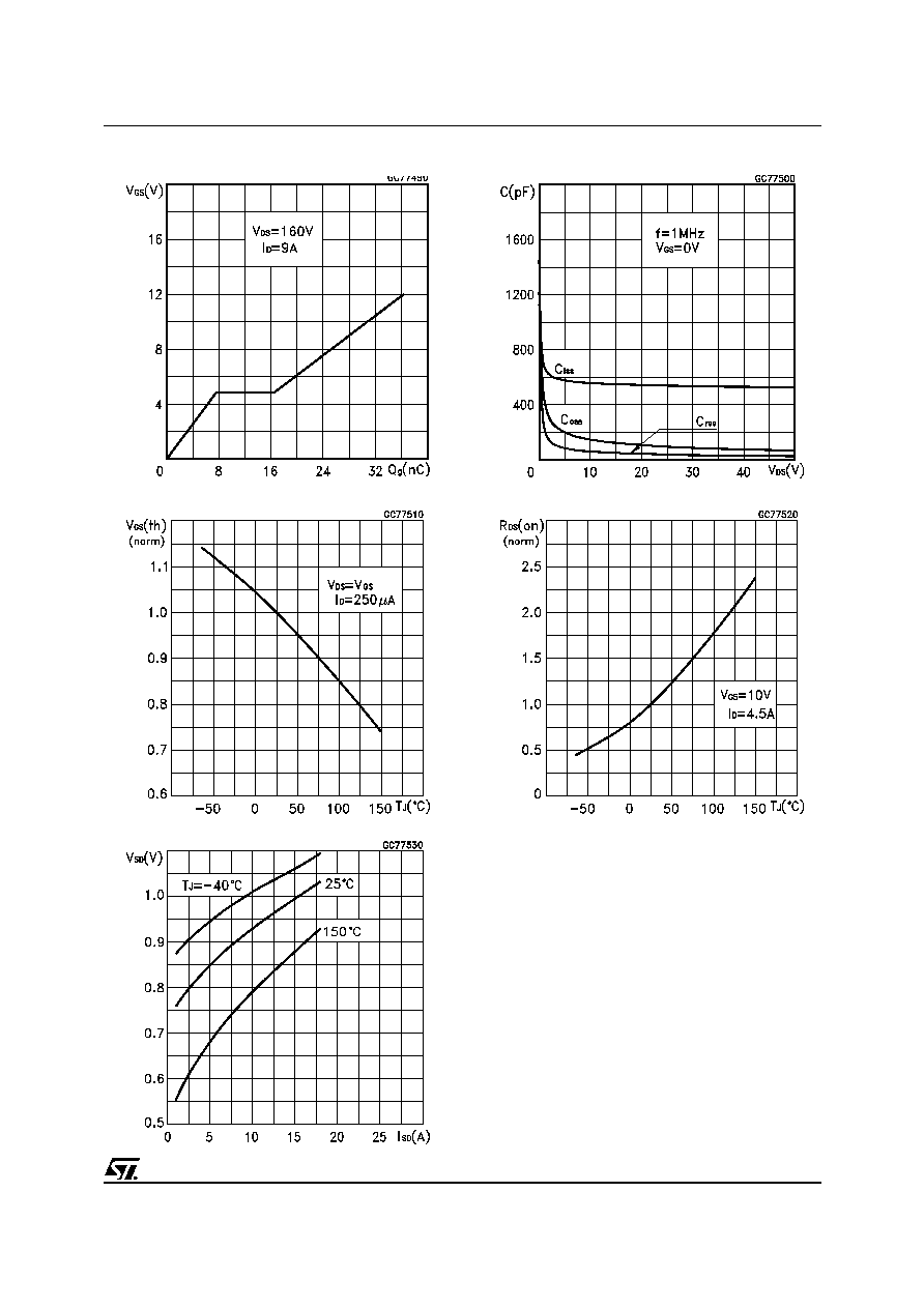
Source-drain Diode Forward Characteristics
Capacitance Variations
Normalized On Resistance vs Temperature
Normalized Gate Threshold Voltage vs Temp.
Gate Charge vs Gate-source Voltage