 | –≠–ª–µ–∫—Ç—Ä–æ–Ω–Ω—ã–π –∫–æ–º–ø–æ–Ω–µ–Ω—Ç: IRF830FI | –°–∫–∞—á–∞—Ç—å:  PDF PDF  ZIP ZIP |
IRF830
N - CHANNEL 500V - 1.35
- 4.5A - TO-220
PowerMESH
TM
MOSFET
s
TYPICAL R
DS(on)
= 1.35
s
EXTREMELY HIGH dv/dt CAPABILITY
s
100% AVALANCHE TESTED
s
VERY LOW INTRINSIC CAPACITANCES
s
GATE CHARGE MINIMIZED
DESCRIPTION
This power MOSFET is designed using the
company's consolidated strip layout-based MESH
OVERLAY
TM
process. This technology matches
and improves the performances compared with
standard parts from various sources.
APPLICATIONS
s
HIGH CURRENT, HIGH SPEED SWITCHING
s
SWITH MODE POWER SUPPLIES (SMPS)
s
DC-AC CONVERTERS FOR WELDING
EQUIPMENT AND UNINTERRUPTIBLE
POWER SUPPLIES AND MOTOR DRIVER
Æ
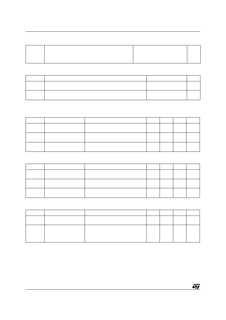
INTERNAL SCHEMATIC DIAGRAM
August 1998
ABSOLUTE MAXIMUM RATINGS
Symbol
Parameter
Value
Unit
V
DS
Drain-source Voltage (V
GS
= 0)
500
V
V
DGR
Drain- gate Voltage (R
GS
= 20 k
)
500
V
V
GS
Gate-source Voltage
±
20
V
I
D
Drain Current (continuous) at T
c
= 25
o
C
4.5
A
I
D
Drain Current (continuous) at T
c
= 100
o
C
2.9
A
I
DM
(
∑
)
Drain Current (pulsed)
18
A
P
tot
Total Dissipation at T
c
= 25
o
C
100
W
Derating Factor
0.8
W/
o
C
dv/dt(
1
)
Peak Diode Recovery voltage slope
3.5
V/ns
T
stg
Storage Temperature
-65 to 150
o
C
T
j
Max. Operating Junction Temperature
150
o
C
(
∑
) Pulse width limited by safe operating area (
1
) I
SD
4.5A, di/dt
75 A/
µ
s, V
DD
V
(BR)DSS
, Tj
T
JMAX
First Digit of the Datecode Being Z or K Identifies Silicon Characterized in this Datasheet
TYPE
V
DSS
R
DS(on)
I
D
IRF830
500 V
< 1.5
4.5 A
1
2
3
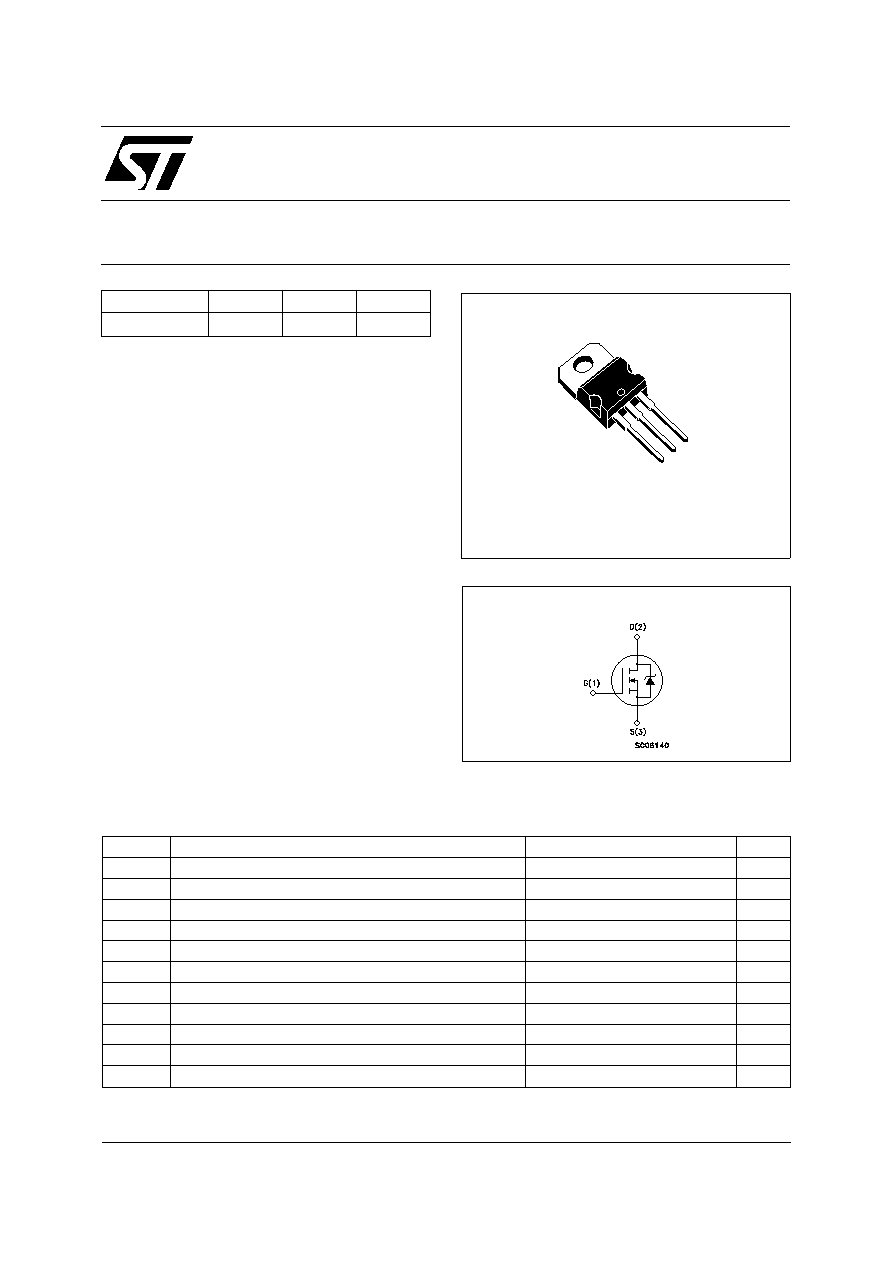
TO-220
1/8
THERMAL DATA
R
thj-case
Rthj-amb
R
thc-sink
T
l
Thermal Resistance Junction-case Max
Thermal Resistance Junction-ambient Max
Thermal Resistance Case-sink Typ
Maximum Lead Temperature For Soldering Purpose
1.25
62.5
0.5
300
o
C/W
oC/W
o
C/W
o
C
AVALANCHE CHARACTERISTICS
Symbol
Parameter
Max Value
Unit
I
AR
Avalanche Current, Repetitive or Not-Repetitive
(pulse width limited by T
j
max)
4.5
A
E
AS
Single Pulse Avalanche Energy
(starting T
j
= 25
o
C, I
D
= I
AR
, V
DD
= 50 V)
290
mJ
ELECTRICAL CHARACTERISTICS (T
case
= 25
o
C unless otherwise specified)
OFF
Symbol
Parameter
Test Conditions
Min.
Typ.
Max.
Unit
V
(BR)DSS
Drain-source
Breakdown Voltage
I
D
= 250
µ
A V
GS
= 0
500
V
I
DSS
Zero Gate Voltage
Drain Current (V
GS
= 0)
V
DS
= Max Rating
V
DS
= Max Rating T
c
= 125
o
C
1
50
µ
A
µ
A
I
GSS
Gate-body Leakage
Current (V
DS
= 0)
V
GS
=
±
20 V
±
100
nA
ON (
)
Symbol
Parameter
Test Conditions
Min.
Typ.
Max.
Unit
V
GS(th)
Gate Threshold
Voltage
V
DS
= V
GS
I
D
= 250
µ
A
2
3
4
V
R
DS(on)
Static Drain-source On
Resistance
V
GS
= 10V I
D
= 2.7 A
1.35
1.5
I
D(on )
On State Drain Current V
DS
> I
D(on)
x R
DS(on)max
V
GS
= 10 V
4.5
A
DYNAMIC
Symbol
Parameter
Test Conditions
Min.
Typ.
Max.
Unit
g
fs
(
)
Forward
Transconductance
V
DS
> I
D(on)
x R
DS(on)max
I
D
= 2.7 A
2.5
S
C
iss
C
oss
C
rss
Input Capacitance
Output Capacitance
Reverse Transfer
Capacitance
V
DS
= 25 V f = 1 MHz V
GS
= 0
610
120
10
pF
pF
pF
IRF830
2/8
ELECTRICAL CHARACTERISTICS (continued)
SWITCHING ON
Symbol
Parameter
Test Conditions
Min.
Typ.
Max.
Unit
t
d(on)
t
r
Turn-on Time
Rise Time
V
DD
= 250 V I
D
= 2.9 A
R
G
= 4.7
V
GS
= 10 V
(see test circuit, figure 3)
11.5
8
ns
ns
Q
g
Q
gs
Q
gd
Total Gate Charge
Gate-Source Charge
Gate-Drain Charge
V
DD
= 400 V I
D
= 3 A V
GS
= 10 V
22
7.2
8
30
nC
nC
nC
SWITCHING OFF
Symbol
Parameter
Test Conditions
Min.
Typ.
Max.
Unit
t
r(Voff)
t
f
t
c
Off-voltage Rise Time
Fall Time
Cross-over Time
V
DD
= 400 V I
D
= 4.5 A
R
G
= 4.7
V
GS
= 10 V
(see test circuit, figure 5)
7
5
15
ns
ns
ns
SOURCE DRAIN DIODE
Symbol
Parameter
Test Conditions
Min.
Typ.
Max.
Unit
I
SD
I
SDM
(
∑
)
Source-drain Current
Source-drain Current
(pulsed)
4.5
18
A
A
V
SD
(
)
Forward On Voltage
I
SD
= 4.5 A V
GS
= 0
1.6
V
t
rr
Q
rr
I
RRM
Reverse Recovery
Time
Reverse Recovery
Charge
Reverse Recovery
Current
I
SD
= 4.5 A di/dt = 100 A/
µ
s
V
DD
= 100 V T
j
= 150
o
C
(see test circuit, figure 5)
435
3.3
15
ns
µ
C
A
(
) Pulsed: Pulse duration = 300
µ
s, duty cycle 1.5 %
(
∑
) Pulse width limited by safe operating area
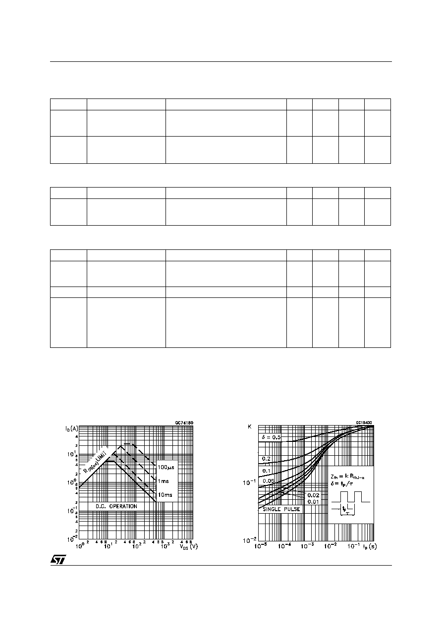
Safe Operating Area
Thermal Impedance
IRF830
3/8
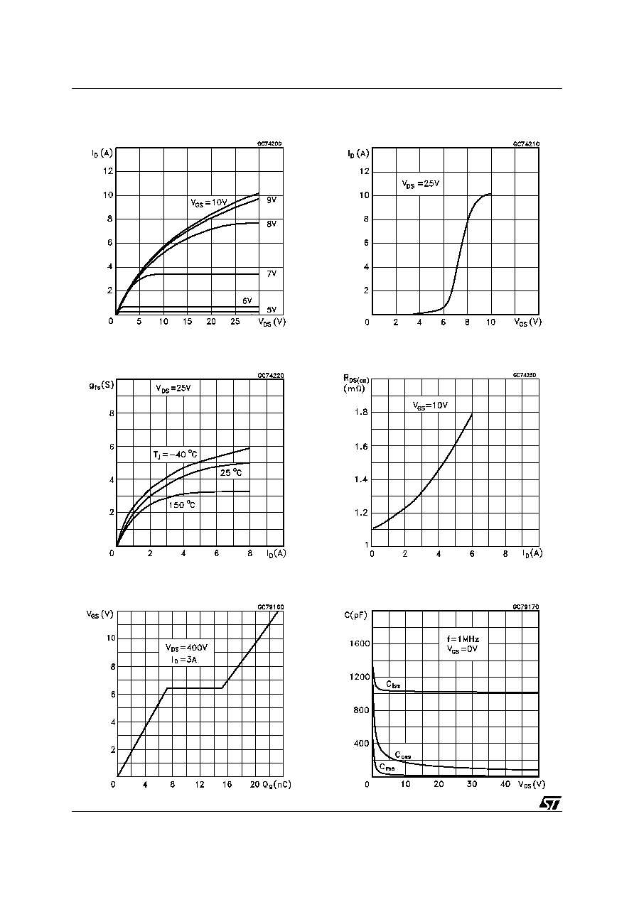
Output Characteristics
Transconductance
Gate Charge vs Gate-source Voltage
Transfer Characteristics
Static Drain-source On Resistance
Capacitance Variations
IRF830
4/8
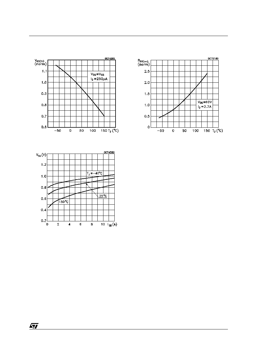
Normalized Gate Threshold Voltage vs
Temperature
Source-drain Diode Forward Characteristics
Normalized On Resistance vs Temperature
IRF830
5/8