 | –≠–ª–µ–∫—Ç—Ä–æ–Ω–Ω—ã–π –∫–æ–º–ø–æ–Ω–µ–Ω—Ç: IRFBC30 | –°–∫–∞—á–∞—Ç—å:  PDF PDF  ZIP ZIP |
IRFBC30
N - CHANNEL 600V - 1.8
- 3.6A - TO-220
PowerMESH
TM
MOSFET
s
TYPICAL R
DS(on)
= 1.8
s
EXTREMELY HIGH dv/dt CAPABILITY
s
100% AVALANCHE TESTED
s
VERY LOW INTRINSIC CAPACITANCES
s
GATE CHARGE MINIMIZED
DESCRIPTION
The PowerMESH
TM
is the evolution of the first
generation of MESH OVERLAY
TM
. The layout
refinements
introduced
greatly
improve
the
Ron*area figure of merit while keeping the device
at the leading edge for what concerns switching
speed, gate charge and ruggedness.
APPLICATIONS
s
HIGH CURRENT, HIGH SPEED SWITCHING
s
SWITH MODE POWER SUPPLIES (SMPS)
s
DC-AC CONVERTERS FOR WELDING
EQUIPMENT AND UNINTERRUPTIBLE
POWER SUPPLIES AND MOTOR DRIVER
Æ
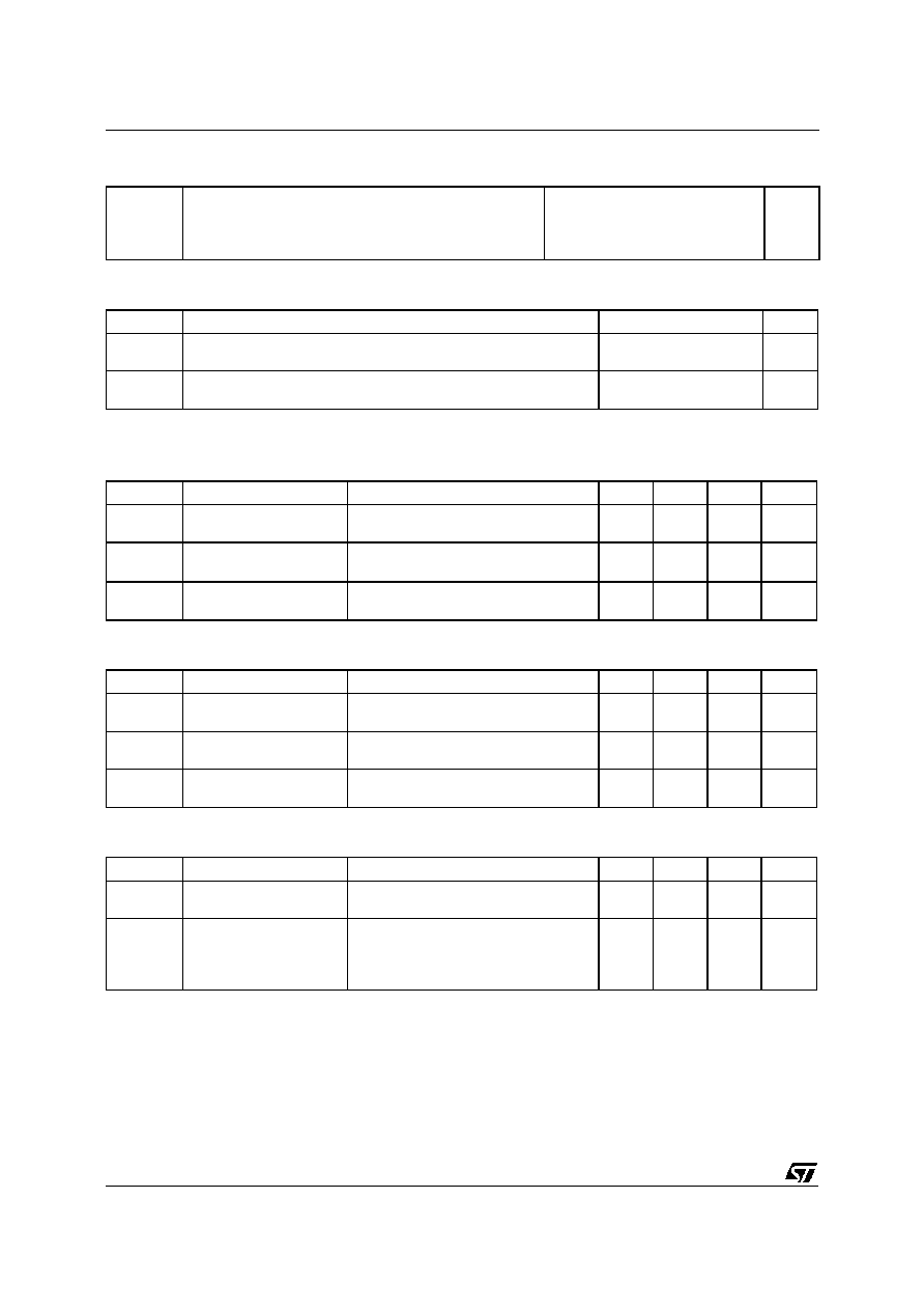
INTERNAL SCHEMATIC DIAGRAM
January 2000
ABSOLUTE MAXIMUM RATINGS
Symbol
Parameter
Value
Un it
V
DS
Drain-source Voltage (V
GS
= 0)
600
V
V
DGR
Drain- gate Volt age (R
GS
= 20 k
)
600
V
V
GS
G ate-source Voltage
±
20
V
I
D
Drain Current (continuous) at T
c
= 25
o
C
3.6
A
I
D
Drain Current (continuous) at T
c
= 100
o
C
2.3
A
I
DM
(
∑
)
Drain Current (pulsed)
14
A
P
tot
T otal Dissipation at T
c
= 25
o
C
75
W
Derating Factor
0.6
W /
o
C
dv/dt (
1
)
Peak Diode Recovery volt age slope
3
V/ns
T
s tg
Storage Temperat ure
-65 to 150
o
C
T
j
Max. Operating Junction Temperature
150
o
C
(
∑
) Pulse width limited by safe operating area
(
1
) I
SD
3.6
A, di/dt
60 A/
µ
s, V
DD
V
(BR)DSS
, Tj
T
JMAX
TYPE
V
DSS
R
DS(on)
I
D
IRFBC30
600 V
< 2.2
3.6 A
1
2
3
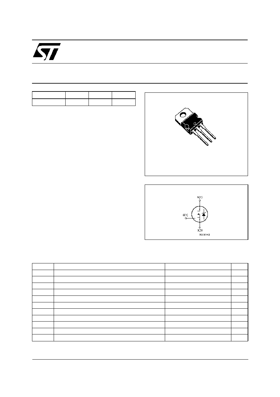
TO-220
1/8
THERMAL DATA
R
thj -case
Rthj -amb
R
thc-sink
T
l
Thermal Resistance Junction-case
Max
Thermal Resistance Junction-ambient
Max
Thermal Resistance Case-sink
Typ
Maximum Lead Temperature For Soldering Purpose
1.7
62.5
0.5
300
o
C/W
oC/W
o
C/W
o
C
AVALANCHE CHARACTERISTICS
Symbo l
Parameter
Max Valu e
Unit
I
AR
Avalanche Current , Repet itive or Not-Repet itive
(pulse width limited by T
j
max)
3. 6
A
E
AS
Single Pulse Avalanche Energy
(starting T
j
= 25
o
C, I
D
= I
AR
, V
DD
= 50 V)
300
mJ
ELECTRICAL CHARACTERISTICS (T
case
= 25
o
C unless otherwise specified)
OFF
Symbo l
Parameter
Test Con ditions
Min.
T yp.
Max.
Unit
V
(BR)DSS
Drain-source
Breakdown Voltage
I
D
= 250
µ
A
V
GS
= 0
600
V
I
DSS
Zero G ate Voltage
Drain Current (V
GS
= 0)
V
DS
= Max Rating
V
DS
= Max Rating
T
c
= 125
o
C
1
50
µ
A
µ
A
I
G SS
Gat e-body Leakage
Current (V
DS
= 0)
V
GS
=
±
20 V
±
100
nA
ON (
)
Symbo l
Parameter
Test Con ditions
Min.
T yp.
Max.
Unit
V
G S(th)
Gat e Threshold
Voltage
V
DS
= V
GS
I
D
= 250
µ
A
2
3
4
V
R
DS(on)
Static Drain-source O n
Resist ance
V
GS
= 10V
I
D
= 2.2 A
1.8
2. 2
I
D(o n)
On Stat e Drain Current
V
DS
> I
D(o n)
x R
DS(on )ma x
V
GS
= 10 V
3. 6
A
DYNAMIC
Symbo l
Parameter
Test Con ditions
Min.
T yp.
Max.
Unit
g
f s
(
)
Forward
Transconduct ance
V
DS
> I
D(o n)
x R
DS(on )ma x
I
D
= 2.2 A
2. 5
S
C
iss
C
os s
C
rss
Input Capacitance
Out put Capacitance
Reverse T ransfer
Capacitance
V
DS
= 25 V
f = 1 MHz
V
GS
= 0
475
72
10
pF
pF
pF
IRFBC30
2/8
ELECTRICAL CHARACTERISTICS (continued)
SWITCHING ON
Symbo l
Parameter
Test Con ditions
Min.
T yp.
Max.
Unit
t
d(on)
t
r
Turn-on Time
Rise Time
V
DD
= 250 V
I
D
= 2.5 A
R
G
= 4.7
V
G S
= 10 V
(see test circuit, figure 3)
14
14
ns
ns
Q
g
Q
gs
Q
gd
Tot al Gate Charge
Gat e-Source Charge
Gat e-Drain Charge
V
DD
= 480 V
I
D
= 3.6 A V
G S
= 10 V
16.5
2.5
9
23. 1
nC
nC
nC
SWITCHING OFF
Symbo l
Parameter
Test Con ditions
Min.
T yp.
Max.
Unit
t
r (Voff)
t
f
t
c
Off -volt age Rise Time
Fall Time
Cross-over Time
V
DD
= 480 V
I
D
= 3.6 A
R
G
= 4.7
V
GS
= 10 V
(see test circuit, figure 5)
15
19
24
ns
ns
ns
SOURCE DRAIN DIODE
Symbo l
Parameter
Test Con ditions
Min.
T yp.
Max.
Unit
I
SD
I
SDM
(
∑
)
Source-drain Current
Source-drain Current
(pulsed)
3. 6
14
A
A
V
SD
(
)
Forward On Volt age
I
SD
= 3. 6A
V
GS
= 0
1. 6
V
t
rr
Q
rr
I
RRM
Reverse Recovery
Time
Reverse Recovery
Charge
Reverse Recovery
Current
I
SD
= 5 A
di/dt = 100 A/
µ
s
V
DD
= 100 V
T
j
= 150
o
C
(see test circuit, figure 5)
600
2.8
9
ns
µ
C
A
(
) Pulsed: Pulse duration = 300
µ
s, duty cycle 1.5 %
(
∑
) Pulse width limited by safe operating area
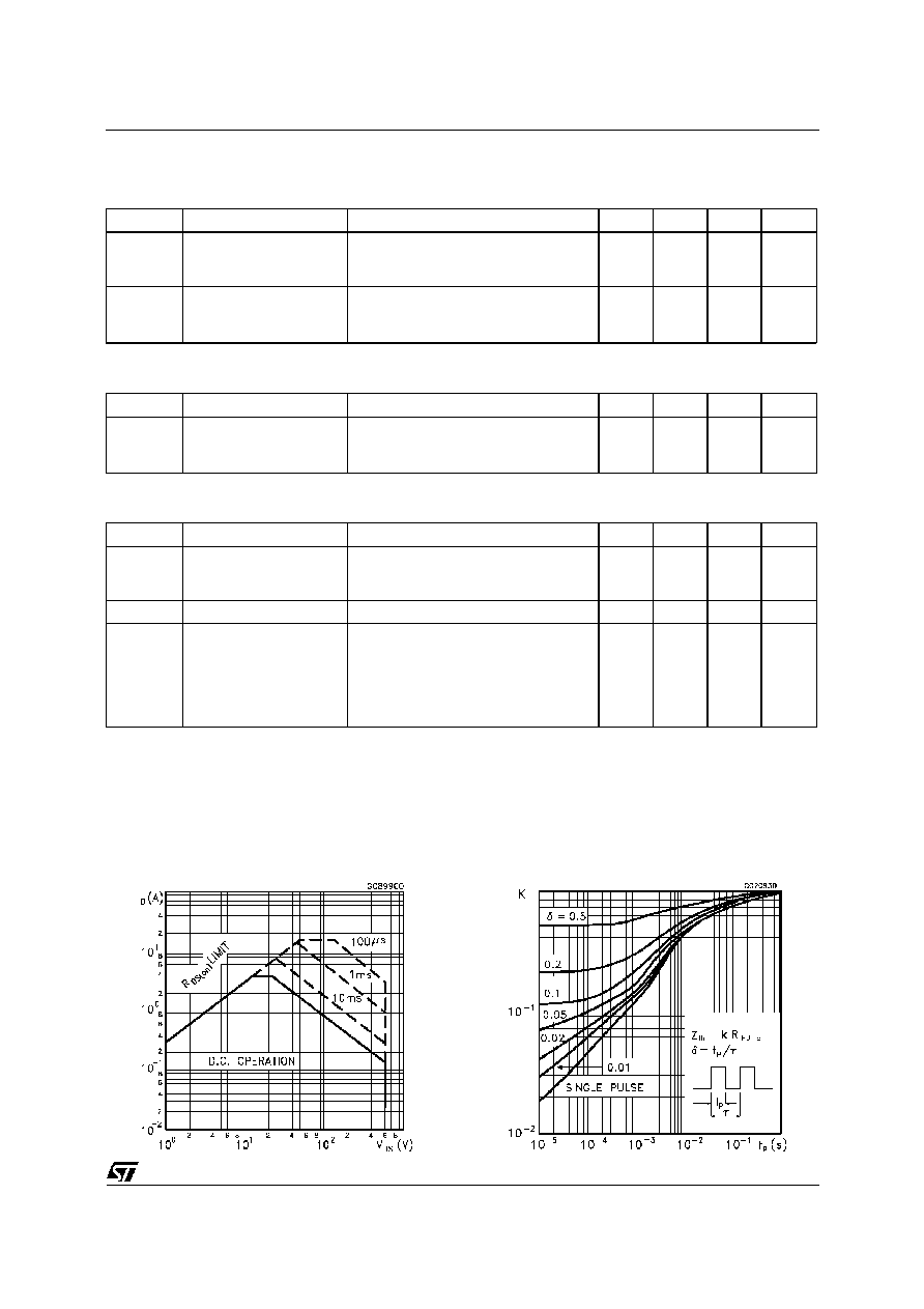
Safe Operating Area
Thermal Impedance
IRFBC30
3/8
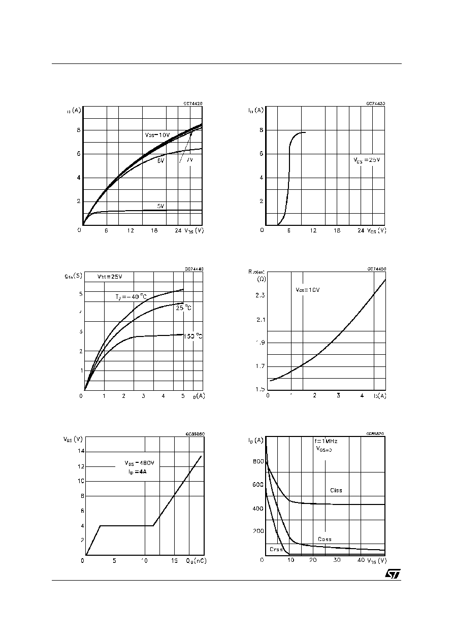
Output Characteristics
Transconductance
Gate Charge vs Gate-source Voltage
Transfer Characteristics
Static Drain-source On Resistance
Capacitance Variations
IRFBC30
4/8
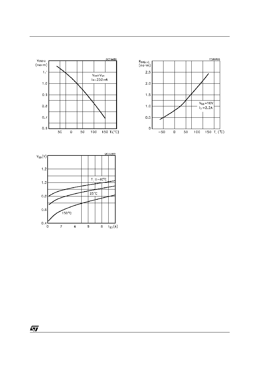
Normalized Gate Threshold Voltage vs
Temperature
Source-drain Diode Forward Characteristics
Normalized On Resistance vs Temperature
IRFBC30
5/8