ISB35000 SERIES
HCMOS STRUCTURED ARRAY
PRELIMINARY DATA
FEATURES
0.5 micron triple layer metal HCMOS process
featuring retrograde well technology, low
resistance salicided active areas, polysilicide
gates and thin metal oxide.
3.3 V optimized transistor with 5 V I/O interface
capability
2 - input NAND delay of 0.210 ns (typ) with
fanout = 2.
Broad I/O functionality including LVCMOS,
LVTTL, GTL, PECL, and LVDS.
High drive I/O; capability of sinking up to 48 mA
with slew rate control, current spike suppression
and impedance matching.
Metallised generators to support SPRAM and
DPRAM, plus an extensive embedded function
library.
Combines Standard Cell Features with Sea of
Gates time to market.
May 1994
F u l ly i n de p en d en t p o we r an d g r oun d
configurations for inputs, core and outputs.
Programmable I/O ring capability up to 1000
pads.
Output buffers capable of driving ISA, EISA,
PCI, MCA, and SCSI interface levels.
Active pull up and pull down devices.
Buskeeper I/O functions.
Oscillators for wide frequency spectrum.
Broad range of 400 SSI cells.
300 element macrofunction library.
Design For Test includes LSSD macro library
option and IEEE 1149.1 JTAG Boundary Scan
architecture built in.
Cadence and Mentor based design system with
interfaces from multiple workstations.
Broad ceramic and plastic package range.
Latchup trigger current +/- 500 mA.
ESD protection +/- 4000 volts.
Internal
Device Name
Total Sites
1
Estimated
2
Gates
Total Usable
3
Gates
Maximum
4
Device Pads
Maximum
5
I/O
ISB35083
124,416
82,944
58,060
188
172
ISB35130
194,400
129,600
90,720
232
216
ISB35166
249,696
166,464
116,524
260
244
ISB35208
311,904
207,936
145,555
288
272
ISB35279
418,176
278,784
195,148
332
316
ISB35389
584,064
389,376
253,094
388
372
ISB35484
726,624
484,416
314,870
432
416
ISB35666
998,784
665,856
399,513
504
488
ISB35832
1,247,616
831,744
499,046
560
544
Notes : 1. Internal sites is based on the number of placement sites available to the route and place software
2. A factor of 1.5 is used to derive the gate complexity from the total available sites. This number is in Nand2 equivalents
3. Factors of 70%, 65%, and 60% have been used to calculate the routing efficiency. This number may vary depending on the
design.
4. 16 corner pads are dedicated to internal and external power supplies. I/O pads may be configured for additional power.
5. Maximum I/O = total device pads minus power pads.
Table 1. Product range
1/15
GENERAL DESCRIPTION
The ISB35000 array series uses a high perform-
ance, low voltage, triple level metal, HCMOS 0.5
micron process to achieve sub-nanosecond inter-
nal speeds while offering very low power dissipation
and high noise immunity. The potential total gate
count ranges above 1 million equivalent usable
gates. The array operates over a Vdd voltage range
of 2.7 to 3.6 volts.
The I/O count for this array family ranges to over
600 signals and 1000 pins dependent upon the
package technology utilized. A Sea of I/O approach
has been followed to give a solution to today's
problems of drive levels and specialized interface
standards. The array does not utilize a set bond pad
spacing but allows for pad spacings from 80 mi-
crons upwards.
The I/O can be configured for circuits ranging from
low voltage CMOS and TTL to 200 mHz plus low
swing differential circuits. Standards like GTL,
SCSI-2, 3.3 Volt PCI, CTI, and a limited set of 5.0
Volt interfaces are currently being addressed. A
specialized set of impedance matched transmis-
sion line driver LVTTL type circuits are also avail-
able with 25, 35, 45, and 55 Ohm output
impedance. These buffers sacrifice direct current
capabilities for matching positive and negative volt-
age and current waveforms.
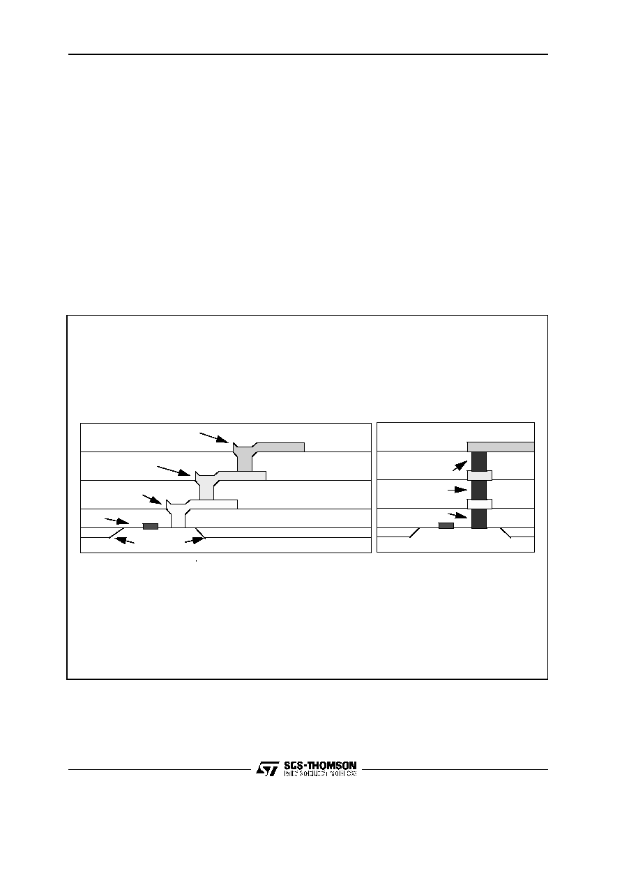
CONVENTIONAL VIA LAYOUT
STACKED VIA LAYOUT
- STACKABLE CONTACTS + VIAs ALLOW MUCH HIGHER DENSITY (AREA SAVINGS UP TO 20% FOR R.L.)
- SIMPLIFIED ROUTING AND DESIGN RULE CHECKING
SUBSTRATE
ISOLATION
GATE
1st DIELECTRIC
2nd DIELECTRIC
CONTACT
CONTACT/VIA
PLUGS
1st
VIA
METAL 1
METAL 2
METAL 3
2nd
VIA
3rd DIELECTRIC
ISB35_VA
Figure 1. Advantages of stacked contacts and vias
ISB35000 SERIES
2/15
TECHNOLOGY OVERVIEW
The design of ISB35000 internal cell is a proprietary
design variation of the CONTINUOUS ARRAY ar-
chitecture previously used in ISB12000, 18000,
and 24000 array families. This proprietary (patent
pending) configuration has been named THE DOU-
BLE BUFFER CELL. This configuration provides a
core that is completely filled with potently active
transistors. Surrounding the core are configura-
tional specialized transistors forming a Sea of I/O
giving a high degree of flexibility to the system
designer. The ISB35000 supports the routing of
signals over unused transistors as needed. Three
levels of metal are utilized, intracell and intercell
wiring are limited to first metal with second and third
metal levels dedicated to interconnect wiring and
power distribution.
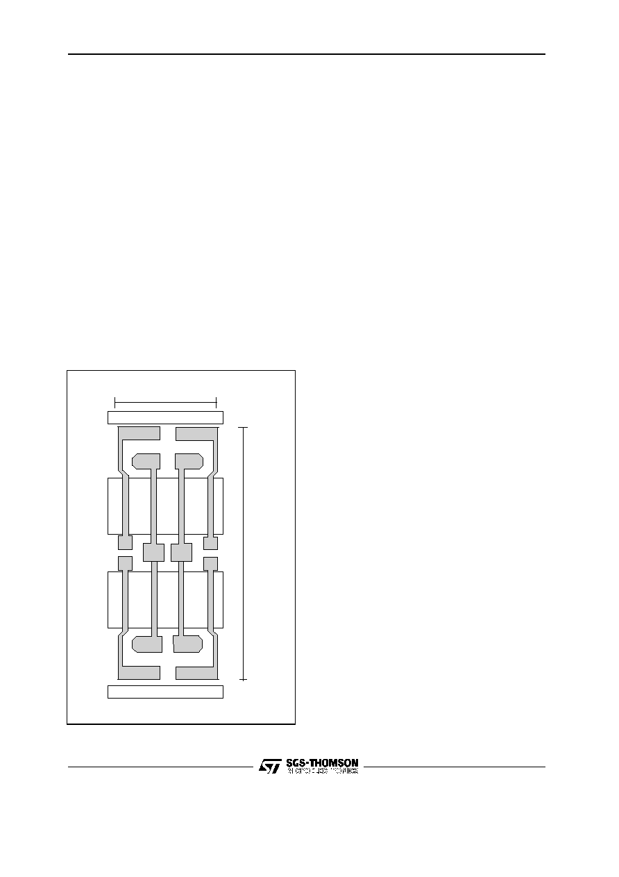
The basic cell is made up of four N and four P type
transistors that are vertically arranged. The centre
two pairs of transistor have common polysilicon
gates, while the outer two pairs have separate
gates for the polysilicon transistors. The cell was
configured to allow extremely high density macro
design for internal macro cell counts over one
million gates while enabling paralleling of transis-
tors to allow high drive capability and the symmetry
of the rise and fall of macro outputs hence the
DOUBLE BUFFER name. Each cell has twelve
horizontal wiring channels on first metal, four verti-
cal wiring channels on second metal and a further
twelve channels on third metal. The HCMOS5 proc-
ess technology allows for adjacent vias and
stacked via1, via2 with or without silicon contacts.
The transistor width utilized by the DOUBLE BUFF-
ER cell is very small as compared to previous
technologies. Even though the basic cell consists
of eight transistors adjacent macros share transis-
tors across the cell borders allowing high density
usage of the resources.
Macros are constructed using resources from one
half cell to tens of cells dependent upon the com-
plexity of the function. The transistors within and
between cells are placed adjacent to each other
sharing source and drain regions. All isolation is
achieved by cutting off adjacent source drain re-
gions with turned off transistors.
A further feature of the Double Buffer cell that helps
allow it to obtain very high density usage is the
proprietary (patent pending) method of localized
power distribution. A major feature of the HCMOS5
process is salicided active areas. This results in
source drain areas that are of one to two ohms
resistance as opposed to the hundreds or thou-
sands of ohms of source drain resistance in pre-
vious technologies. This very low resistance is one
reason that very low transistor widths could be
utilized in the cell design since drive is not lost due
to source drain resistance. This use of low width
transistors results in lower capacitance loading of
the gates due to the smaller areas utilized. Low
resistance, low capacitance, and small gates re-
sults in low power usage for inverters as compared
to previous ISB technologies. This reduction in
power allows the use of salicided active stripes for
power distribution replacing the first level metal
buses used in previous technologies. This removal
of the metal one power buses simplified macro
layout allowing additional wiring resources to be left
for the router allowing a higher density usage of the
array than would be achievable with previous
power distribution techniques. One other gain in the
performance of the array and its usability for the
customer was derived from the use of the salicided
10 �m
30 �m
ISB35_PA
Figure 2. Internal Core Cell
ISB35000 SERIES
3/15
active power distribution. Since the power distribu-
tion serves as the well ties the inherent capacitance
of the reversed biased well junctions is closely
coupled into the power distribution and functions as
localized decoupling capacitance helping to keep
high frequency noise from being coupled from one
macro to the other through the power distribution.
The salicided active local distribution of the DOU-
BLE BUFFER cell is supplied its power by a screen
grid of power bused on both second and third metal.
The second metal buses run every nine cells and
are two wiring tracks wide. Vss and Vdd is inter-
leaved every other bus. The third level buses run
every thirty six tracks and are three tracks wide. This
grid is sufficient to power all but the largest arrays
though the use of custom structured cores or gate
counts above 500,000 usable cells along with high
clock rates may result in the need for supplemental
power. The overall die power distribution is broken
down into a minimum of three Vdd and three Vss
distributions. Optionally other distributions for spe-
cialized I/O may be inserted. The standard distribu-
tions are Internal Vdd and Vss, serving the internal
cells and the prebuffer sections of the I/O, External
Vdd and Vss serving the output transistors only, and
Receiver Vdd and Vss serving the first stages of the
receiver cells. Optional distributions for 5.0V inter-
face, GTL, CTL, and other standards can be utilized
as necessary.
LIBRARY
The following section details the elements which
make up the ISB35000 Series library. The elements
are organised into three categories:
1. Macrocell library with Input, Output, Bidirectional
Buffers including JTAG macrocells and Core
cells.
2. Macrofunctions
3. Module generators
4. Embedded Functions
I/O BUFFERS
ISB35000 technology does not utilize a standard
type I/O cell but is a leader in the emerging Sea of
I/O approach to handling the chip interface problem.
This approach starts at the bond pad area of the I/O
where the pad size and pitch is not determined until
the customers choice of packaging, signal interface
standards and I/O count is considered. Wire bond
pad spacings for 80 micron centres are available
where large signal counts are most important.
Pad spacing can be increased incrementally. It is
expected that most designs will use 100 or 120
micron spacings. It is also possible to use different
spacings for different width output sections when
needed within the same device.
Along with the variable bond pad spacing the I/O
output transistor section does not have a fixed
width. Previous technologies utilized a design ap-
proach where the desired full function buffer was
designed for a maximum current taking one pad
location with the usual current in the range of twenty
four milliamps. The approach followed in ISB35000
is to have identical twenty micron wide output tran-
sistor slices stepped around the die. Each slice
contains one set of protection diodes to the external
power rails and eight P and eight N transistors. The
transistors are specifically laid out and selectively
non salicided for ESD protection and latch up pre-
vention. These slices are paralleled to meet the
current needs of the user, for example, to construct
a 24mA sink and 12mA source LVTTL buffer, a
number of slices would be used. The next group of
devices that makes up the I/O circuits is again a 20
u wide slice of specialized transistors that are util-
ized to form the slew rate control sections of the I/O.
Each of these slices has circuits to control the
switching of up two sections of P and N output
transistors. These sections are of course created
from the output transistor slice above the slew rate
section and can be connected as desired by the
designer. Many configurations of circuits can be
created to supply the desired results with slew rate
slices paralleled with multiple output sections. A
further function of the scan circuits is current spike
suppression during switching of the I/O transistors.
The logic utilized causes the conducting transistors
to turn off before the opposing set of transistors turn
on.
Inside the slew rate sections the next slices of
specialized designed components step on a 40
micron wide pattern. The first of these 40 micron
wide sections is utilized for predriver circuits; these
include specialized built in test functions for the I/O.
The predriver of course interfaces the core signals
controlling tristate and switching functions with the
slew rate and output transistor sections but it also
allows all Output Buffers to be driven high, low or
put into tristate regardless of the state of the internal
logic greatly simplifying parametric testing of the
part and also assisting customers who wish to use
this feature during board testing. Note that all output
ISB35000 SERIES
4/15
buffers can be tristated by this function including
buffers that normally do not tristate. This test func-
tion also turns off all pull up or down devices and
shuts down all differential receivers and converts
them into standard CMOS receivers. Inside the
predriver is a section of specialized transistors used
to create the receiver functions. This section in-
cludes specialized non salicide protection resistor
diodes to further protect the gates of the receiver
devices from ESD and latch up. Also present in this
section are devices that can be utilized to form
various parameteriseable pull up, pull down and
buskeeper functions. A full set of standard receivers
with pull up and pull down devices is present in the
library. The technologies supported match the out-
put buffer capabilities and include, LVCMOS,
LVTTL, GTL, CTL, Differential, etc. and a five volt
interface capability. The last section of devices that
make up the I/O ring is a set of custom designed
(for compactness) scan latches and supporting cir-
cuits that can be utilized to form various types of
scan circuits conforming to the standard that the
customer is utilizing in his systems. These circuits
can be combined with internal transistors if needed.
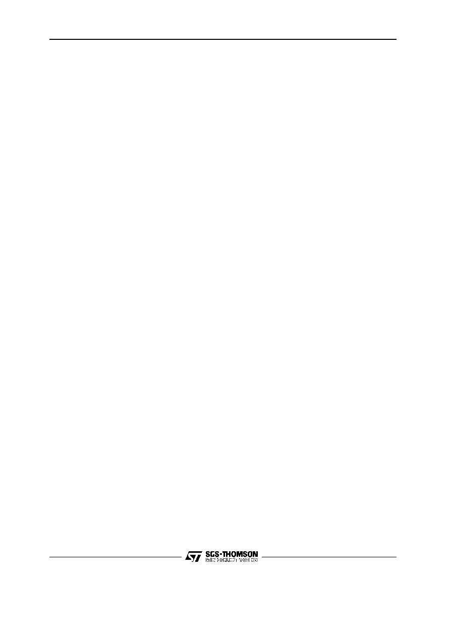
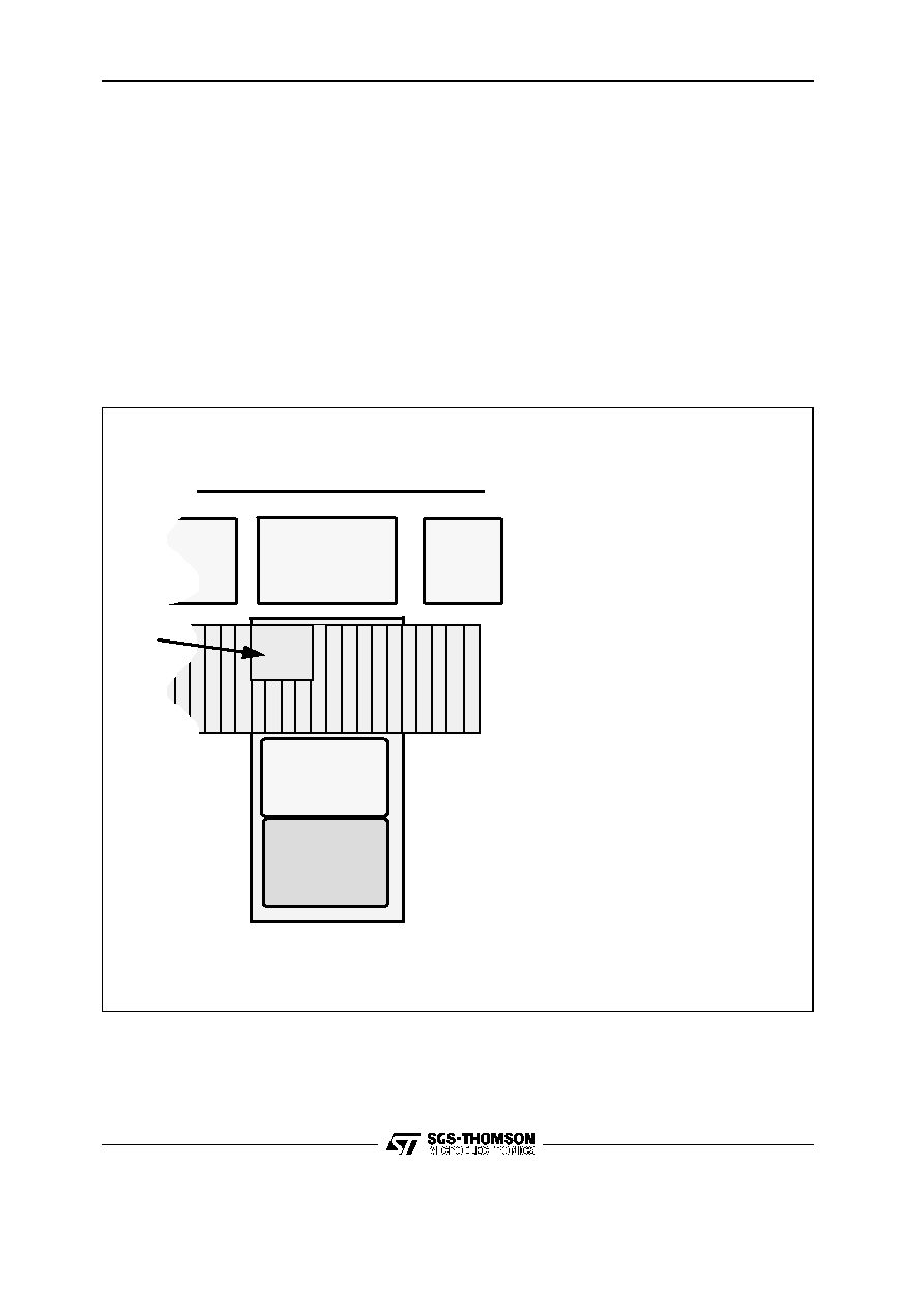
Programmable
Pitch Bond
Pad
Input &
Control
SlewRate
Tristate
Buskeeper
Level Shifter
JTAG
Guardring
Die Core
Edge of Die
4mA
selected
Segmented
Output
River of Drive
Transistors
ISB35_PB
Figure 3. ISB35000 I/O Technology
ISB35000 SERIES
5/15