 | –≠–ª–µ–∫—Ç—Ä–æ–Ω–Ω—ã–π –∫–æ–º–ø–æ–Ω–µ–Ω—Ç: ITA10C1 | –°–∫–∞—á–∞—Ç—å:  PDF PDF  ZIP ZIP |
MONOLITHIC TRANSIL
Æ
ARRAY FOR DATA LINE PROTECTION
IN ACCORDANCE WITH :
- ESD standard :
. IEC 801-2
15kV
5ns / 50ns
. IEC 801-4
40A
5ns / 50ns
. IEC 801-5
1kV
1.2 / 50
µ
s
25A
8 / 20
µ
s
. MIL STD 883C - Method 3015-2
V
P
= 25kV
C = 150pF
R = 150
5 s duration
- Human body test :
V
P
= 4kV
C = 150pF
R = 150
FEATURES
HIGH SURGE CAPABILITY TRANSIL ARRAY
I
PP
= 40 A 8/20
µ
s
UP TO 5 BIDIRECTIONAL TRANSIL FUNC-
TIONS
BREAK DOWN VOLTAGE AND MAXIMUM DIF-
FERENTIAL
VOLTAGE
BETWEEN
TWO
INPUT PINS :
ITA6V5 = 6.5 V
ITA10 = 10 V
ITA18 = 18 V
ITA25 = 25 V
LOW CLAMPING FACTOR (V
CL
/ V
BR
) AT HIGH
CURRENT LEVEL
LOW LEAKAGE CURRENT
LOW INPUT CAPACITANCE
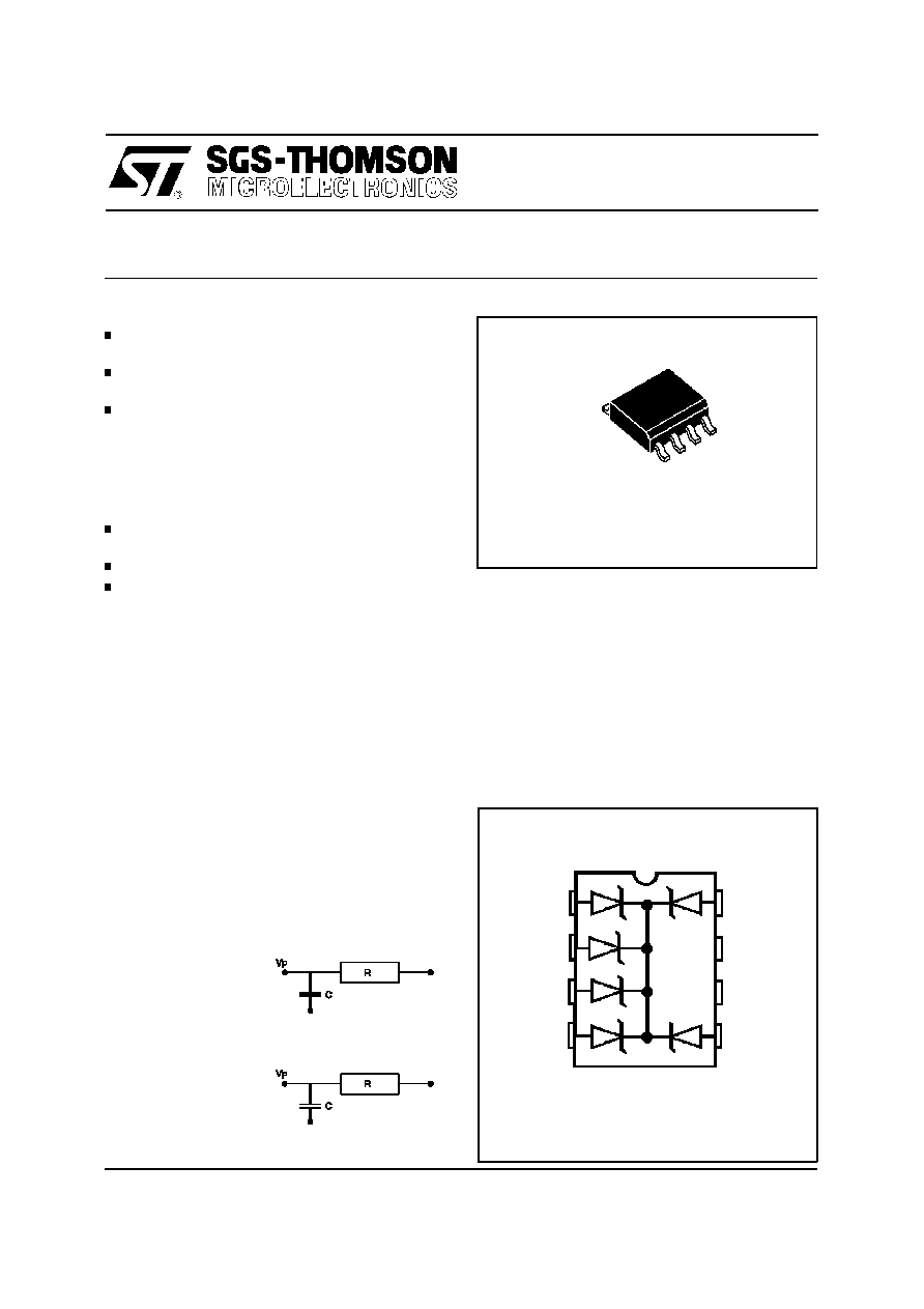
SO8
FUNCTIONAL DIAGRAM
DESCRIPTION
This is a specific transil array for RS232, RS423 in-
terface protection developed in monolithic chip
form in order to provide a high surge capability and
a low clamping voltage
EQUIVALENT TO 4 BIDIRECTIONAL TRANSILS
5 GND
6
7
8 GND
April 1998 - Ed: 3
I/04 4
I/03 3
I/02 2
I/01 1
ITA6V5C1 / ITA10C1
ITA18C1 / ITA25C1
1/5
Symbol
Parameter
Value
Unit
I
PP
Peak pulse current for 8/20
µ
sexponential
pulse
See note
40
A
I
2
t
Wire I
2
t value
See note
0.6
A
2
s
T
stg
T
j
Storage and Junction Temperature Range
- 55 to + 150
125
∞
C
∞
C
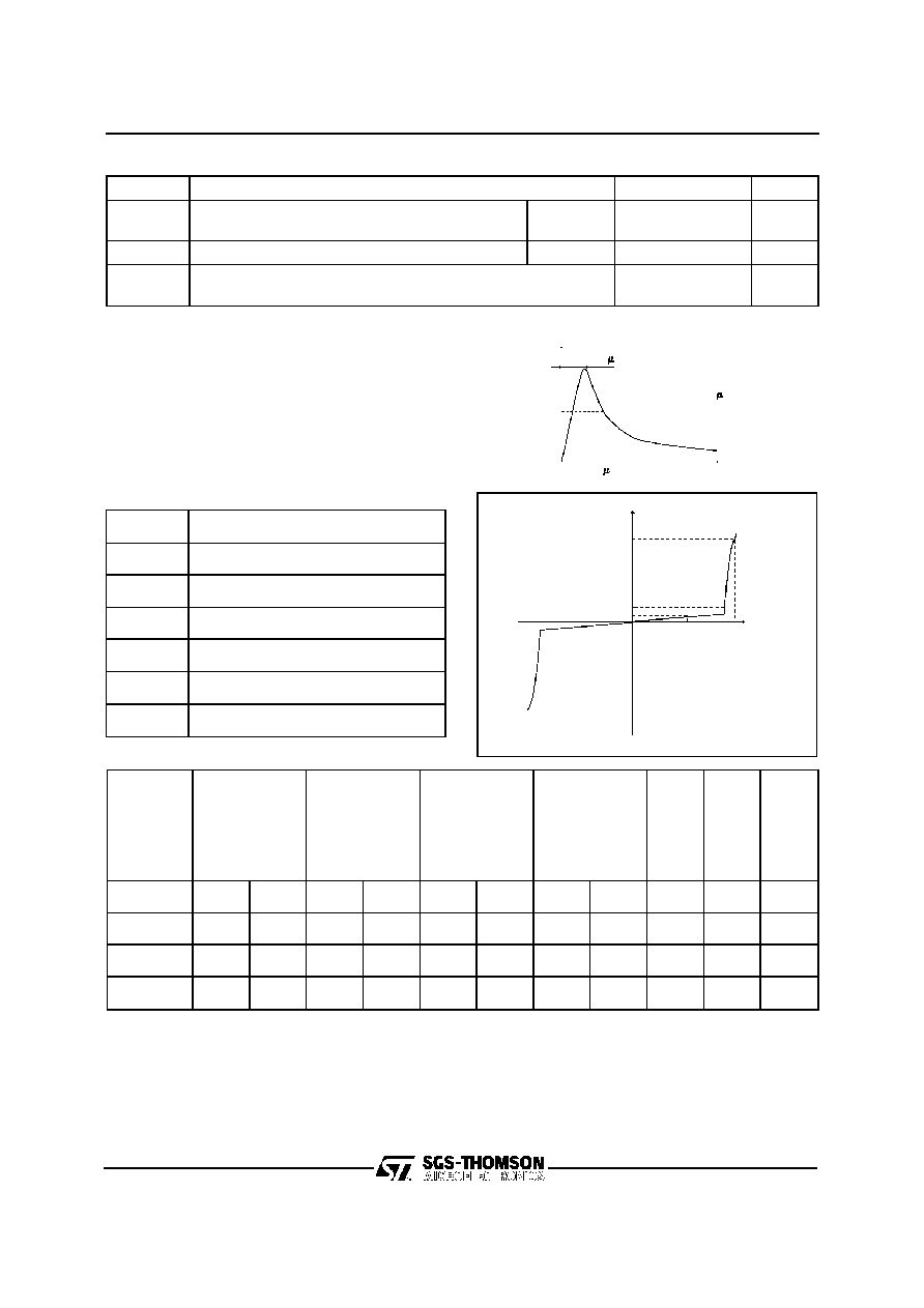
ABSOLUTE RATINGS (limiting values) (0
∞
C
Tamb
70
∞
C)
Note :
For surges greater than the maximum value specified, the
input/output will present first a short circuit to the common
bus line and after an open circuit caused by the wire.
V CL
VBR
V RM
I
R
IRM
I PP
I
V
Symbol
Parameter
I
RM
Leakage Current @ V
RM
V
RM
Stand-off Voltage
V
BR
Breakdown Voltage
V
CL
Clamping Voltage
I
PP
Surge Current
C
Input Capacitance
ELECTRICAL CHARACTERISTICS
Types
I
RM
@
V
RM
V
BR
@
I
R
V
CL
@
I
PP
V
CL
I
PP
C 1
C 2
T
max
min
8/20
µ
s
max
8/20
µ
s
max
max
max
Note 1
Note 1
Note 1
Note 2
Note 3
µ
A
V
V
mA
V
A
V
A
pF
pF
10
-4
/
∞
C
ITA6V5C1
10
5
6.5
1
10
10
12
25
750
550
4
ITA10C1
10
8
10
1
15
10
19
25
570
260
8
ITA18C1
4
15
18
1
25
10
28
25
350
180
9
ITA25C1
4
24
25
1
33
10
38
25
300
100
12
All parameters tested at 25
∞
C, except where indicated.
Note 1: Between I/O pin and ground.
Note 2: Between two input Pins at 0 V Bias.
Note 3: Between two input Pins at V
RM
.
100
50
0
20
s
t
%I pp
8
s
Pu lse wave for m 8/20 s
ITA6V5C1/ ITA10C1 / ITA18C1 / ITA25C1
2/5
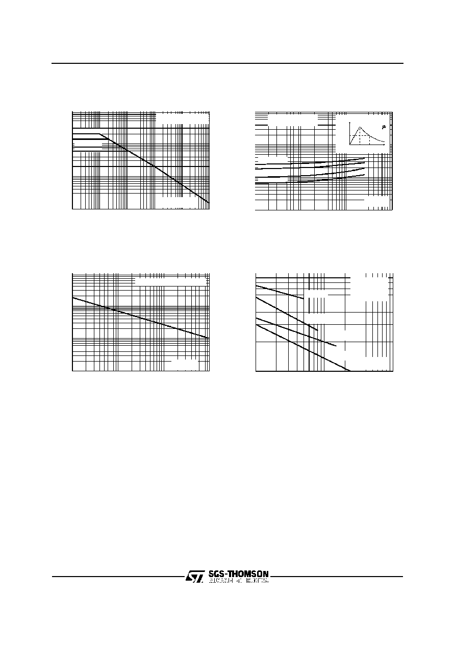
Note :
The curve of the figure 2 is specified for a junction temperature of 25
∞
C before surge.
P
(W)
1E-03
1E-02
1E-01
1E+00
1E+01
1E+02
1E+01
1E+02
1E+03
1E+04
ITA25C1
ITA18C1
ITA10C1
ITA6V5C1
T
initial = 25 C
j
o
t
(ms) expo
P
P
Fig.1 : Typical Peak pulse power versus exponen-
tial pulse duration.
I
(A)
1E-02
1E-01
1E+00
1E+01
1E+00
1E+01
1E+02
1E+03
DC
exponential waveform
t
(ms)
Fig.3 : Peak current I
DC
inducing open circuit of the
wire for one input/output versus pulse duration
(typical values).
C (pF)
1E+00
1E+01
1E+02
1E+02
1E+03
T
= 25 C
f = 1 MHz
j
o
V
(V)
R
ITA18C1
ITA25C1
ITA10C1
ITA6V5C1
Fig.4 : Junction capacitance versus reverse ap-
plied voltage for one input/output (typical values).
V
(V)
1E-01
1E+00
1E+01
1E+02
1E+00
1E+01
1E+02
1E+03
CL
I
(A)
PP
T
initial = 25 C
j
o
PP
% I
t
t
t
r
t = 8
s
r
100
50
0
ITA25C1
ITA18C1
ITA10C1
ITA6V5C1
Fig.2 : Clamping voltage versus peak pulse cur-
rent exponentialwaveform 8/20
µ
s.
ITA6V5C1 / ITA10C1 / ITA18C1 / ITA25C1
3/5
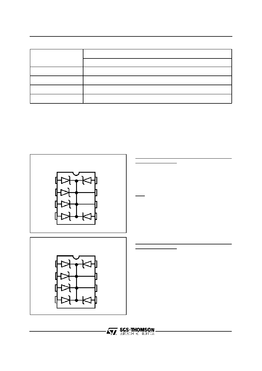
Fig 5 : EQUIVALENT TO 4 BIDIRECTIONAL TRANSILS
UTILIZATION AS A BIDIRECTIONAL TRANSIL
ARRAY WITH 4 I/Os.
The main applicationof this device is to be configu-
rated as a 4, bidirectional Transil Array as per the
Pin-out of Fig 5.
Pins 5 and 8 are connected to ground.
INPUTS/OUTPUTS are from Pin 1 to Pin 4.
Note : The bidirectional functionis made with 2 uni-
directional Transils. One (T1) is connected to the
INPUT/OUTPUT, the other one (T2) is connected
to the ground (see Fig 5).
Ground is connected via 2 diodes T2 and T3 .
This allows to withstand 2 specified surges on 2 dif-
ferent lines at the same time.
UTILIZATION AS A BIDIRECTIONAL TRANSIL
ARRAY WITH 5 I/Os.
The ITAxxC1 can be used as a 5 bidirectional
Transil Array.
Ground can be connected to any pin (except 6 and
7).
The other pins are used as INPUTS and OUT-
PUTS.
The bidirectional function is made with 2 unidirec-
tional Transils T1 and T2. One example with
ground on Pin 8 is shown in Fig 6.
This configuration allows to withstand only one
specified surge at the same time.
INSTRUCTION GUIDE
This monolithic Transil Array is based on 6 Unidirectional Transils with a common cathode and can be con-
figurated to offer 4 or 5 bidirectional functions, according to the following customer application.
I/O4 4
I/O3 3
I/O2 2
I/O1 1
5 GND
6
7
8 GND
T2
T1
T3
Fig 6 : EQUIVALENT TO 5 BIDIRECTIONAL TRANSILS
I/O4 4
I/O3 3
I/O2 2
I/O1 1
5 I/O5
6
7
8 GND
T2
T1
Types
Maximum differential voltage between two input pins at 25
∞
C
V
ITA6V5C1
6.5
ITA10C1
10
ITA18C1
18
ITA25C1
25
APPLICATION NOTICE
ITA6V5C1/ ITA10C1 / ITA18C1 / ITA25C1
4/5
ORDER CODE
ITA
25 C 1
INTEGRATED
TRANSIL ARRAY
V
BR
min
PACKAGE
1=SO8 PLASTIC
COMMON GROUND
TYPE
ITA6V5C1
ITA10C1
ITA18C1
ITA25C1
MARKING
6V5C1
10C1
18C1
25C1
MARKING
Information furnished is believed to be accurate and reliable. However, SGS-THOMSON Microelectronics assumes no responsibility for the
consequences of use of such information nor for any infringement of patents or other rights of third parties which may result from its use. No
license is granted by implication or otherwise under any patent or patent rights of SGS-THOMSON Microelectronics. Specifications mentioned
in this publication are subject to change without notice. This publication supersedes and replaces all information previously supplied.
SGS-THOMSON Microelectronics products are not authorized for use as critical components in life support devices or systems without express
written approval of SGS-THOMSON Microelectronics.
©
1998 SGS-THOMSON Microelectronics - Printed in Italy - All rights reserved.
SGS-THOM SON Microelectronics GROUP OF COMPANIES
Australia - Brazil - Canada - China - France - Germany - Italy - Japan - Korea - Malaysia - Malta - Morocco
The Netherlands - Singapore - Spain - Sweden - Switzerland - Taiwan - Thailand - United Kingdom - U.S.A.
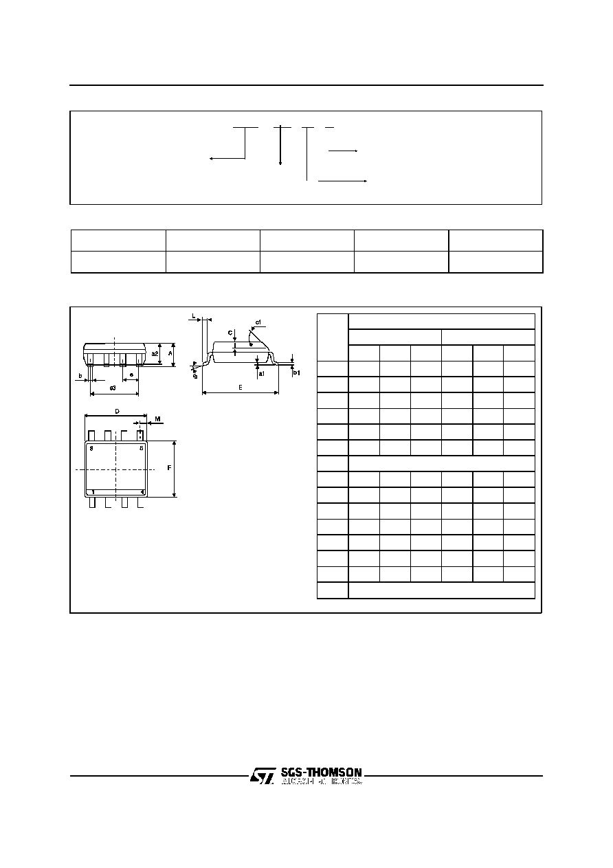
PACKAGE MECHANICAL DATA
SO8
Weight : 0.077g
REF.
DIMENSIONS
Millimetres
Inches
Min.
Typ. Max. Min.
Typ. Max.
A
1.75
0.069
a1
0.1
0.25 0.004
0.010
a2
1.65
0.065
b
0.35
0.48 0.014
0.019
b1
0.19
0.25 0.007
0.010
C
0.50
0.020
c1
45
∞
(typ)
D
4.8
5.0
0.189
0.197
E
5.8
6.2
0.228
0.244
e
1.27
0.050
e3
3.81
0.150
F
3.8
4.0
0.15
0.157
L
0.4
1.27 0.016
0.050
M
0.6
0.024
S
8
∞
(max)
ITA6V5C1 / ITA10C1 / ITA18C1 / ITA25C1
5/5