 | –≠–ª–µ–∫—Ç—Ä–æ–Ω–Ω—ã–π –∫–æ–º–ø–æ–Ω–µ–Ω—Ç: ITA6V1U1 | –°–∫–∞—á–∞—Ç—å:  PDF PDF  ZIP ZIP |
1/5
ITA6V1U1
Æ
August 2001- Ed: 2
TRANSIL
TM
ARRAY
FOR DATALINE PROTECTION
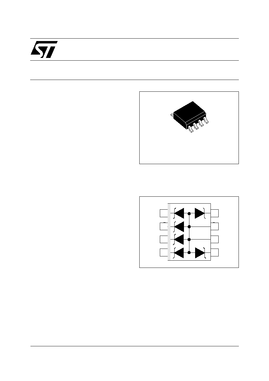
SO-8
Data transmission lines protection :
- Unipolar signal up to 5.5V
- Bipolar signal in the +/- 2.5V range
APPLICATIONS
Application Specific Discretes
A.S.D.
TM
1
2
3
4
I/O1
I/O 2
I/O 3
I/O 4
G N D
G N D
8
7
6
5
I/O6
I/O 5
FUNCTIONAL DIAGRAM
s
HIGH SURGE CAPABILITY TRANSIL ARRAY
I
PP
= 40 A (8/20
µ
s)
s
PEAK PULSE POWER : 300 W (8/20
µ
s)
s
UP TO 6 UNIDIRECTIONAL TRANSIL FUNC-
TIONS
s
LOW CLAMPING FACTOR (V
CL
/ V
BR
) AT
HIGH CURRENT LEVEL
s
LOW LEAKAGE CURRENT
s
ESD PROTECTION UP TO 15kV
FEATURES
Transil diode arrays
provide high overvoltage
protection by clamping action. Their instantaneous
response to transient overvoltages makes them
particularly suited to protect voltage sensitive
devices such as MOS Technology and low voltage
supplied IC's.
The ITA series allies high surge capability against
energetic pulses with high voltage performance
against ESD.
DESCRIPTION
IEC 1000-4-2 : level 4
IEC 1000-4-4 : level 4
IEC 1000-4-5 : level 2
MIL STD 883C - Method 3015-6 : class 3
(human body model)
COMPLIES WITH THE FOLLOWING STANDARDS :
ITA6V1U1
2/5
Symbol
Parameter
V
RM
Stand-off voltage
V
BR
Breakdown voltage
V
CL
Clamping voltage
I
RM
Leakage current @ V
RM
I
PP
Peak pulse current
T
Voltage temperature coefficient
C
Junction capacitance
V
F
Forward voltage drop
ELECTRICAL CHARACTERISTICS (T
amb
= 25∞C)
V CL VBR
V RM
I
I F
V F
IRM
I PP
Symbol
Parameter
Value
Unit
P
PP
Peak pulse power dissipation (8/20
µ
s)
(see note 1)
Tj initial = T
amb
300
W
I
PP
Peak pulse current (8/20
µ
s) (see note 1)
Tj initial = T
amb
40
A
I
2
t
Wire I
2
t value (see note 1)
0.6
A
2
s
T
stg
T
j
Storage temperature range
Maximum operating junction temperature
- 55 to + 150
125
∞C
∞
C
T
L
Maximum lead temperature for soldering during 10s
260
∞
C
ABSOLUTE MAXIMUM RATINGS (T
amb
= 25∞C)
Note 1 : For surges greater than the specified maximum
value, the I/O will first present a short-circuit and after an
open circuit caused by the wire melting.
100
50
0
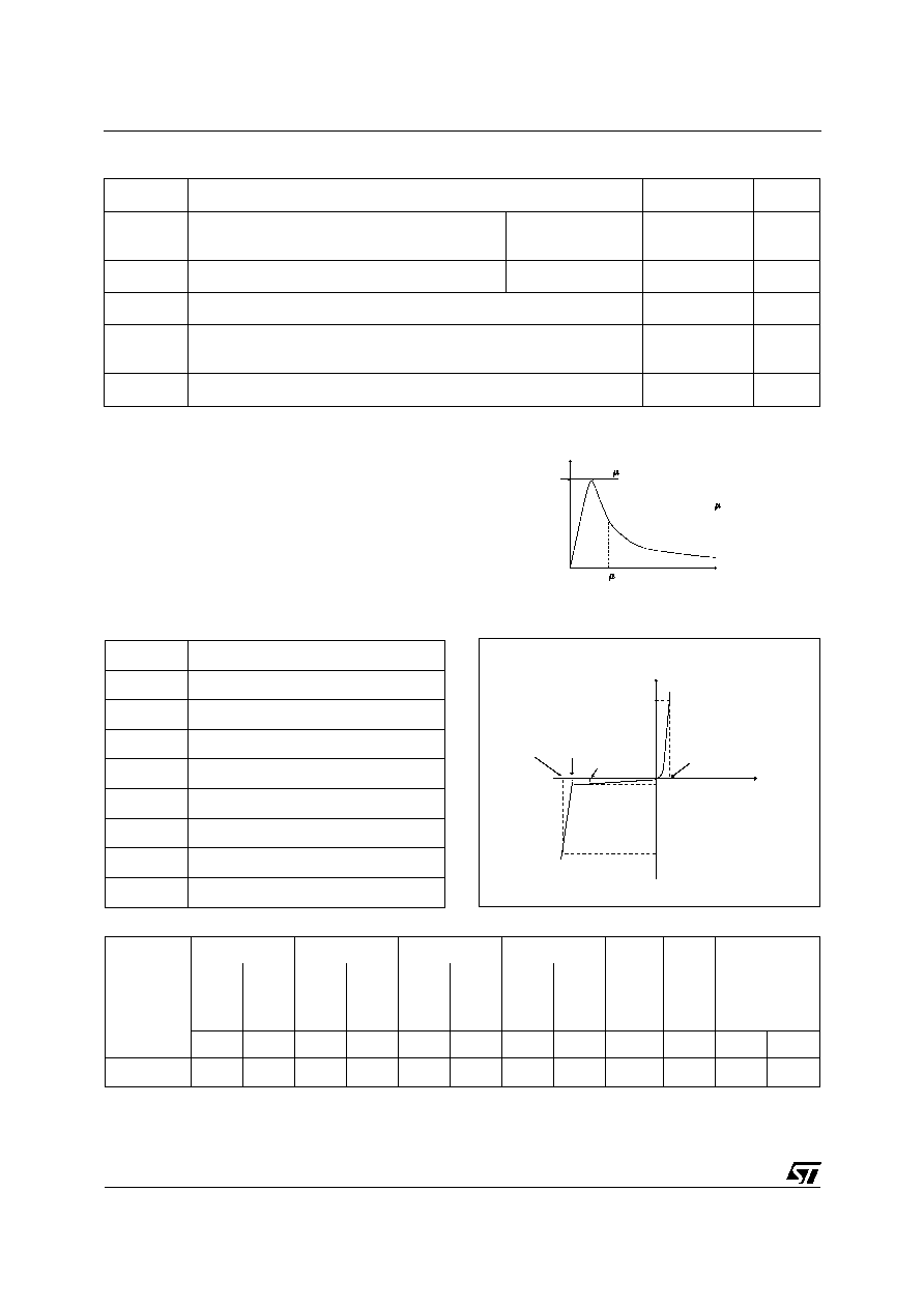
20 s
t
%I pp
8 s
Pulse wave form 8/20
s
Types
I
RM
@
V
RM
V
BR
@
I
R
V
CL
@
I
PP
V
CL
@
I
PP
T
C
V
F
@
I
F
max.
min.
max.
8/20
µ
s
max.
8/20
µ
s
max.
max.
max.
note 2
note 2
note 2
note 3
µ
A
V
V
mA
V
A
V
A
10
-4
/∞C
pF
V
A
ITA6V1U1
10
5
6.1
1
10
10
12
25
4
1500
1.3
1
Note 2 : Between I/O pin and ground.
Note 3 : Between I/O pin and ground, at 0V Bias. F = 1MHz.
ITA6V1U1
3/5
1E-3
1E-2
1E-1
1E+0
1E+1
10
100
1000
Ppp(W)
T
initial = 25 C
j
o
tp (ms) expo
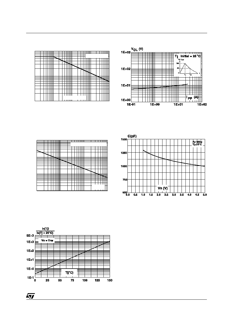
Fig. 1 : Typical peak pulse power versus
exponential pulse duration.
I
(A)
1E-02
1E-01
1E+00
1E+01
1E+00
1E+01
1E+02
1E+03
DC
exponential waveform
t (ms)
Fig. 3 : Peak current I
DC
inducing open circuit of
the wire for one input/output versus pulse duration
(typical values).
Fig. 4 : Junction capacitance versus reverse
applied voltage for one input/output (typical
values).
Fig.
2 : Clamping voltage versus peak pulse
current (exponential waveform 8/20
µ
s).
Fig. 5 : Relative variation of leakage current
versus junction temperature
ITA6V1U1
4/5
ITA 6V1 U 1 RL
Integrated
Transil Array
V
min
BR
Unidirectional
Packaging:
RL = Tape & reel
= Tube
Package: SO-8 Plastic
ORDER CODE
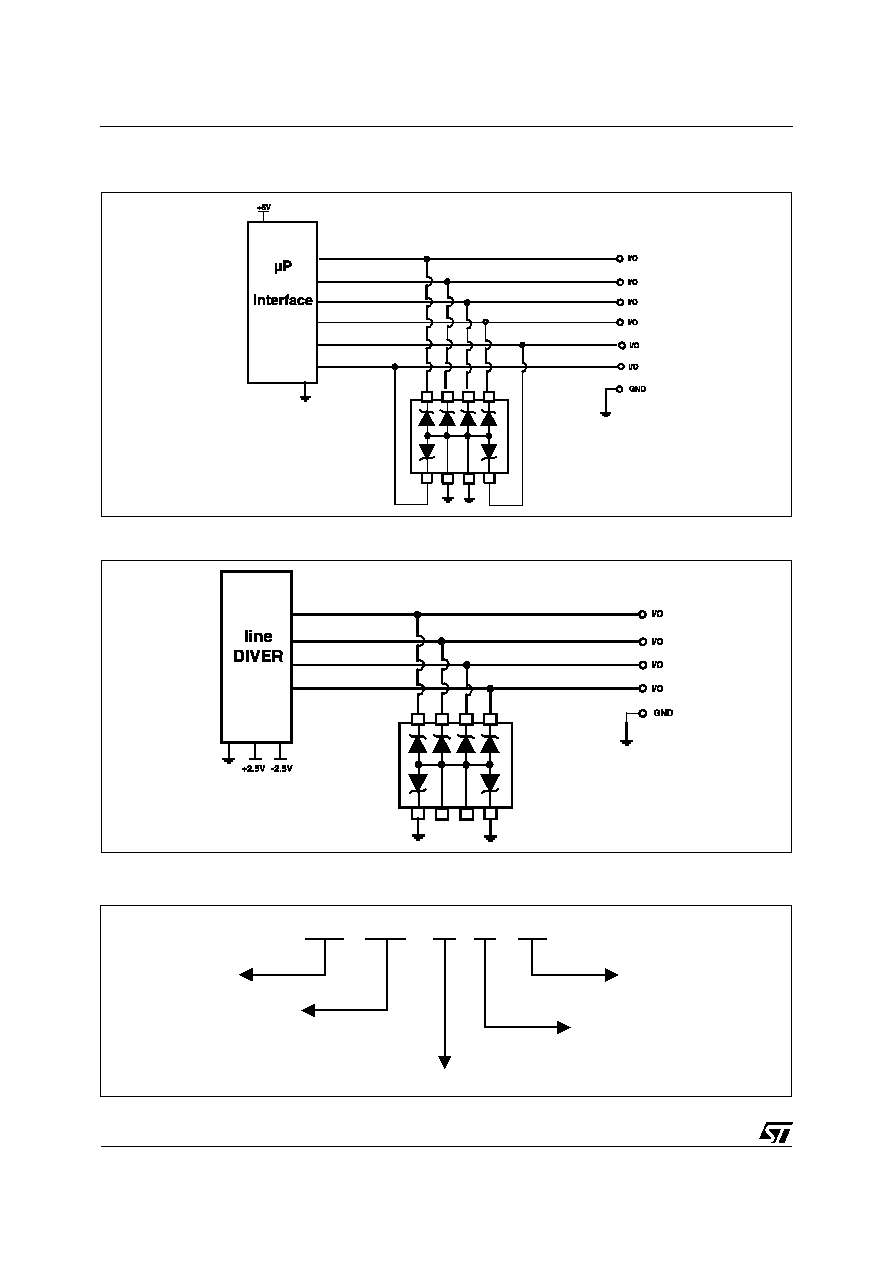
APPLICATION INFORMATION
Typical application 1 :
µ
P I/O lines
Typical application 2 : +/-2.5V Data lines
ITA6V1U1
5/5
TYPE
MARKING
ITA6V1U1
6V1U1
MARKING
Information furnished is believed to be accurate and reliable. However, STMicroelectronics assumes no responsibility for the consequences of
use of such information nor for any infringement of patents or other rights of third parties which may result from its use. No license is granted by
implication or otherwise under any patent or patent rights of STMicroelectronics. Specifications mentioned in this publication are subject to
change without notice. This publication supersedes and replaces all information previously supplied.
STMicroelectronics products are not authorized for use as critical components in life support devices or systems without express written ap-
proval of STMicroelectronics.
The ST logo is a registered trademark of STMicroelectronics
© 2001 STMicroelectronics - Printed in Italy - All rights reserved.
STMicroelectronics GROUP OF COMPANIES
Australia - Brazil - China - Finland - France - Germany - Hong Kong - India - Italy - Japan - Malaysia
Malta - Morocco - Singapore - Spain - Sweden - Switzerland - United Kingdom - U.S.A.
http://www.st.com
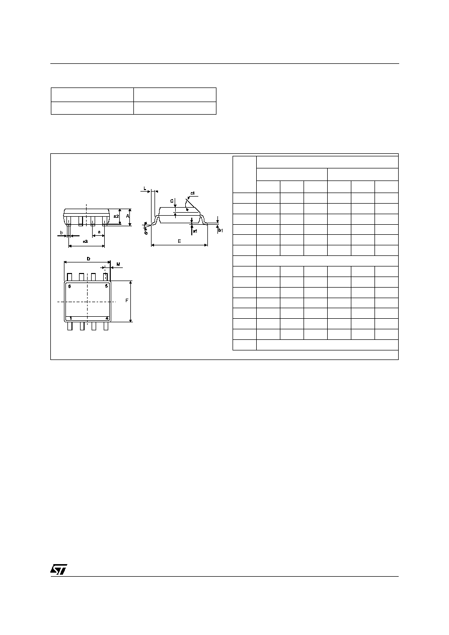
PACKAGE MECHANICAL DATA
SO-8 (Plastic)
REF.
DIMENSIONS
Millimetres
Inches
Min.
Typ.
Max.
Min.
Typ.
Max.
A
1.75
0.069
a1
0.1
0.25 0.004
0.010
a2
1.65
0.065
b
0.35
0.48 0.014
0.019
b1
0.19
0.25 0.007
0.010
C
0.50
0.020
c1
45∞ (typ)
D
4.8
5.0
0.189
0.197
E
5.8
6.2
0.228
0.244
e
1.27
0.050
e3
3.81
0.150
F
3.8
4.0
0.15
0.157
L
0.4
1.27 0.016
0.050
M
0.6
0.024
S
8∞ (max)
Packaging : Preferred packaging is tape and reel.
Weight : 0.08g.