 | –≠–ª–µ–∫—Ç—Ä–æ–Ω–Ω—ã–π –∫–æ–º–ø–æ–Ω–µ–Ω—Ç: ITAXXU1 | –°–∫–∞—á–∞—Ç—å:  PDF PDF  ZIP ZIP |
Æ
1/6
ITAxxU1
TRANSILTM ARRAY
FOR DATALINE PROTECTION
REV. 1
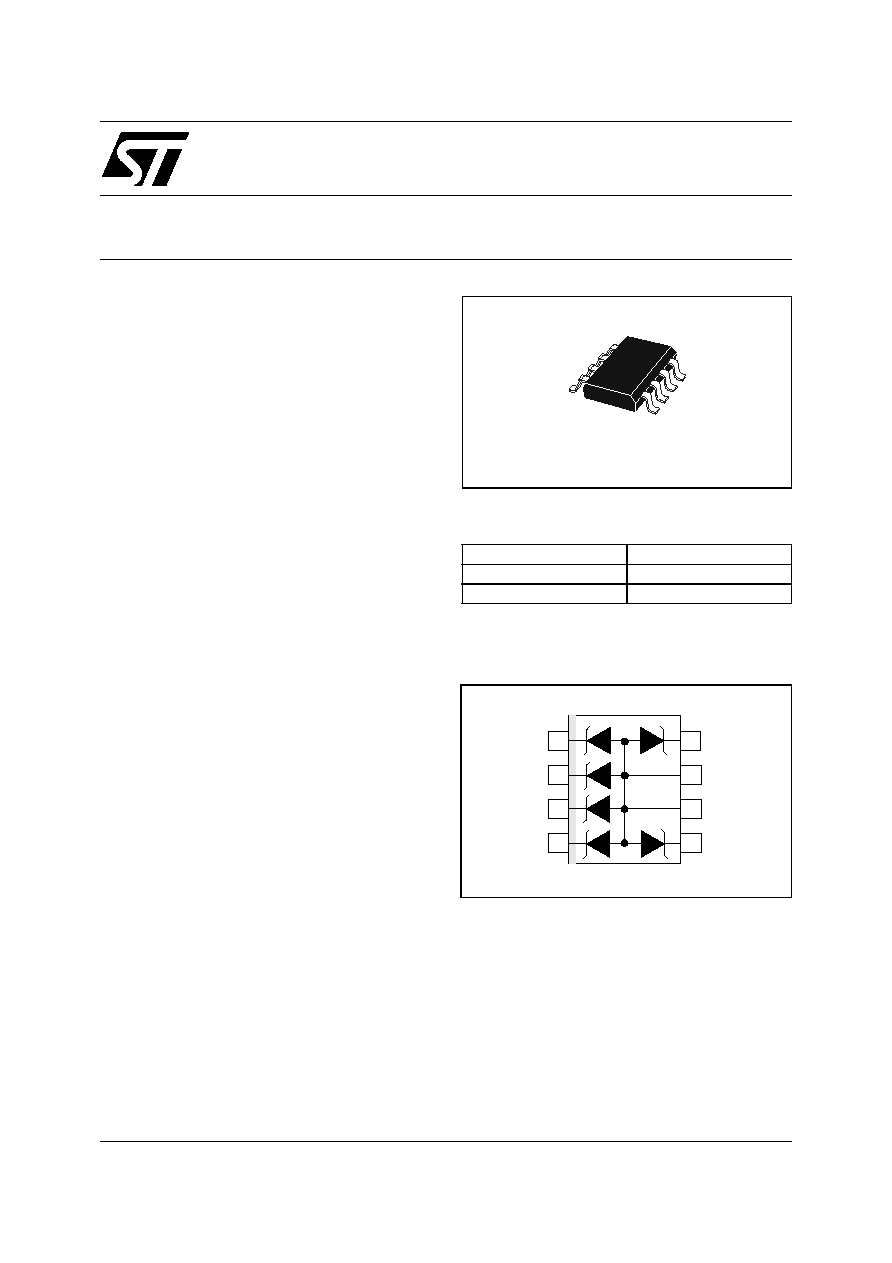
SO-8
December 2004
MAIN APPLICATIONS
Data transmission lines protection, such as :
Unipolar signal up to 5.5 V
Bipolar signal in the ± 2.5 V range
FEATURES
High surge capability Transil array:
I
PP
= 40 A (8/20µs)
Peak pulse power : 300 W (8/20µs)
Up to 6 bidirectional Transil functions
Low clamping factor (V
CL
/ V
BR
) at high current
level
Low leakage current
ESD protection up to 15kV
DESCRIPTION
Transil diode arrays provide high overvoltage pro-
tection by clamping action. Their instantaneous re-
sponse to transient overvoltages makes them
particularly suited to protect voltage sensitive de-
vices such as MOS Technology and low voltage
supplied IC's.
The ITA series allies high surge capability against
energetic pulses with high voltage performance
against ESD.
COMPLIES WITH THE FOLLOWING STANDARDS:
IEC61000-4-2 level 4:
15kV (air discharge)
8kV
(contact discharge)
MIL STD 883E-Method 3015-7: class3
25kV HBM (Human Body Model)
Table 1: Order Codes
Part Number
Marking
ITA6V1U1
6V1U1
ITA6V1U1RL
6V1U1
ASDTM
Figure 1: Functional Diagram
1
2
3
4
I/O1
I/O2
I/O3
I/O4
GND
GND
I/O5
I/O6
8
7
6
5
TM: ASD and TRANSIL are trademarks of STMicroelectronics.
ITAxxU1
2/6
Table 2: Absolute Ratings (T
amb
= 25∞C)
Table 3: Electrical Characteristics (T
amb
= 25∞C)
Symbol
Parameter
Value
Unit
P
PP
Peak pulse power (8/20µs) (see note 1)
T
j
initial = T
amb
300
W
I
PP
Peak pulse current (8/20µs) (see note 1)
T
j
initial = T
amb
40
A
I
2
t
Wire I
2
t value (see note 1)
0.6
A
2
s
T
j
Maximum operating junction temperature
125
∞C
T
stg
Storage temperature range
-55 to +150
∞C
T
L
Maximum lead temperature for soldering during 10 s at 5mm for case
260
∞C
Note 1: For surges greater than the specified maximum value, the I/O will first present a short-circuit and after an open circuit caused by
the wire melting.
Symbol
Parameter
V
RM
Stand-off voltage
V
BR
Breakdown voltage
V
CL
Clamping voltage
I
RM
Leakage current
I
PP
Peak pulse current
T
Voltage temperature coefficient
V
F
Forward voltage drop
C
Capacitance
Part
Number
V
BR
@ I
R
I
RM
@ V
RM
V
CL
@ I
PP
V
CL
@ I
PP
T
C
V
F
@ I
F
min.
max.
max.
8/20µs
max.
8/20µs
max.
max.
max.
note 2
note 2
note 2
note 3
V
mA
µA
V
V
A
V
A
10
-4
/∞C
pF
V
A
ITA6V1U1
6.51
1
10
5
10
10
12
25
4
1500
1.3
1
Note 2: Between I/O pin and ground.
Note 3: Between two input pins at 0V Bias, F = 1 MHz.
V
CL
V
BR
V
RM
V
F
I
F
I
RM
I
PP
I
V
ITAxxU1
3/6
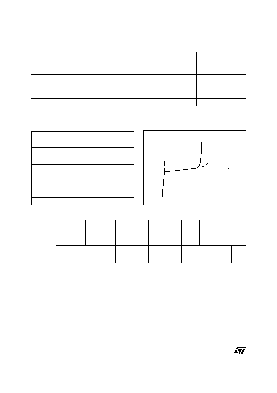
Figure 2: Pulse waveform
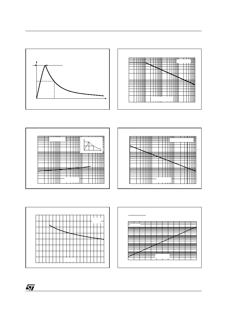
Figure 3: Typical peak pulse power versus
exponential pulse duration
Figure 4: Clamping voltage versus peak pulse
current (exponential waveform 8/20µs)
Figure 5: Peak current I
DC
inducing open
circuit of the wire for one input/output versus
pulse duration (typical values)
Figure 6: Junction capacitance versus reverse
applied voltage for one input/output (typical
values)
Figure 7: Relative variation of leakage current
versus junction temperature
%I
PP
t
8µs
100
50
0
20µs
Pulse waveform 8/20µs
1E-3
1E-2
1E-1
1E+0
1E+1
10
100
1000
P
PP
(W)
T
j
initial=25∞C
t
P
(ms) expo
V
CL
(V)
T
j
initial=25∞C
I
PP
(A)
1E+00
1E+01
1E+02
1E+03
1E-01
1E+00
1E+01
1E+02
%I
PP
t
r
100
50
0
t
p
t
I
DC
(A)
t
P
(ms)
1E+00
1E+01
1E+02
1E+03
1E-02
1E-01
1E+00
1E+01
Exponential waveform
0.0
0.5
1.0
1.5
2.0
2.5
3.0
3.5
4.0
4.5
5.0
500
750
1000
1250
1500
C(pF)
V
R
(V)
T
j
=25∞C
F=1MHz
5E+3
1E+3
1E+2
1E+1
0
25
50
75
100
125
150
1E+0
1E-1
T
j
(∞C)
I
R
(T )
I (T =25∞C)
j
R
j
V
R
=V
RM
ITAxxU1
4/6
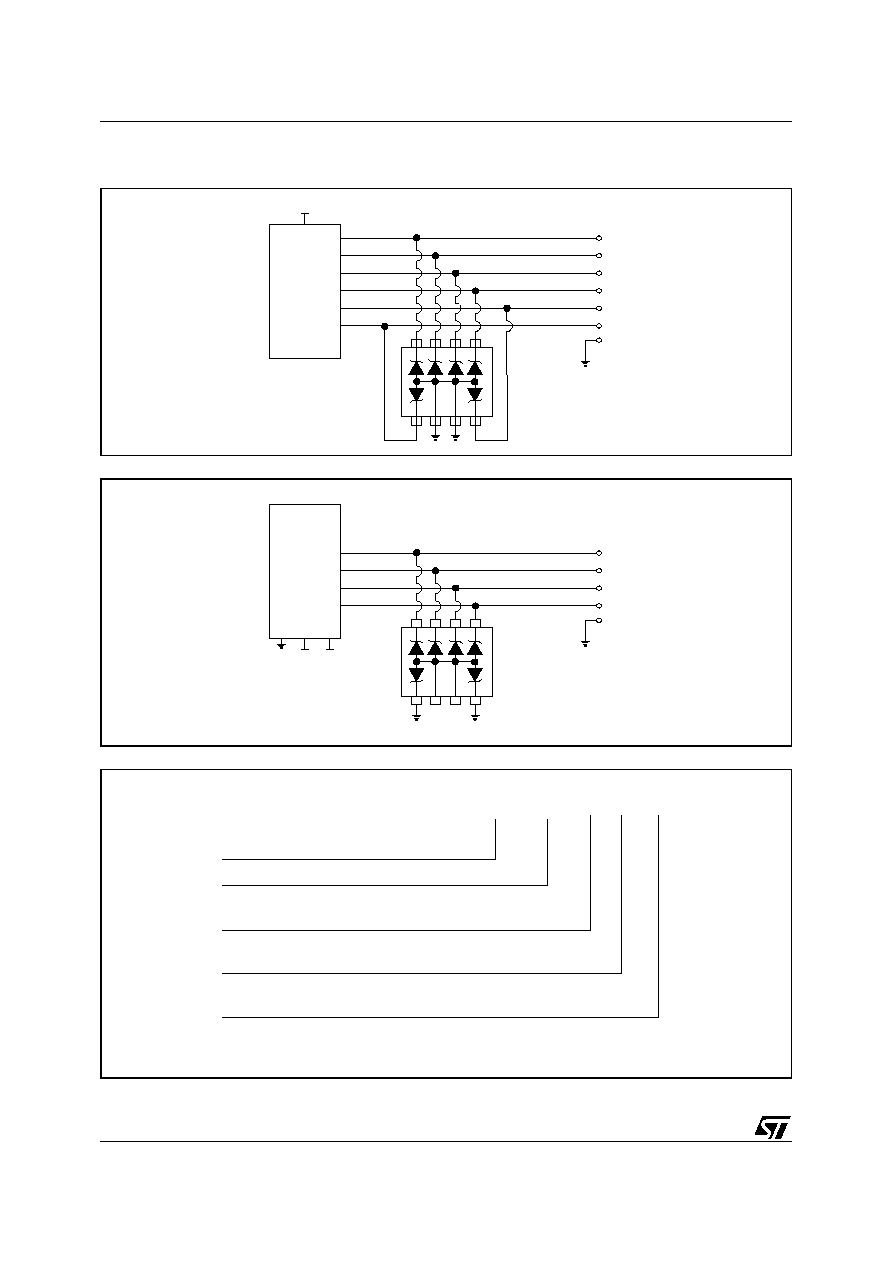
APPLICATION INFORMATION
Figure 8: µP I/O lines
Figure 9: ± 2.5V datalines
Figure 10: Ordering Information Scheme
GND
µP
interface
I/O
I/O
I/O
I/O
I/O
I/O
+5V
GND
Line
driver
I/O
I/O
I/O
I/O
+2.5V -2.5V
ITA 6V1 U 1 RL
Integrated Transil Array
Breakdown Voltage (min)
Type of lines protected
Package
Packaging
25 = 25 Volt
U = Unidirectional
1 = SO-8
RL = Tape & reel
Blank = Tube
ITAxxU1
5/6
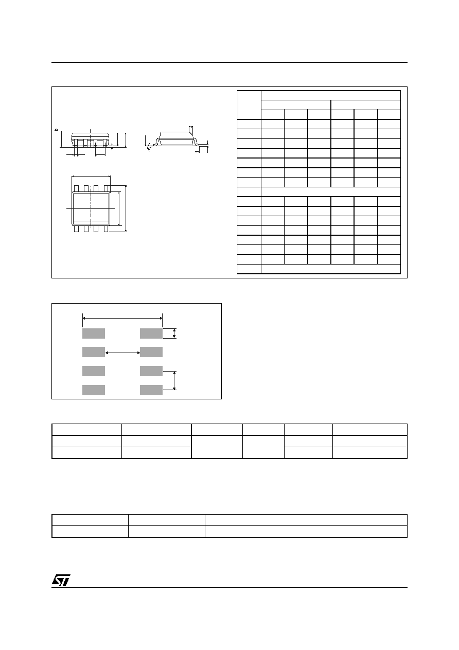
Figure 11: SO-8 Package Mechanical Data
Figure 12: Foot Print Dimensions (in millimeters)
E
D
8
4
1
5
H
k
h x 45∞
L
C
(Seating
Plane)
0.25mm
(Gage Plane)
e
A
A2
B
A1
ddd C
6.8
4.2
1.27
0.6
Table 4: Ordering Information
Part Number
Marking
Package
Weight
Base qty
Delivery mode
ITA6V1U1
6V1U1
SO-8
0.08 g
2000
Tube
ITA6V1U1RL
6V1U1
2500
Tape & reel
Table 5: Revision History
Date
Revision
Description of Changes
13-Dec-2004
1
First issue
REF.
DIMENSIONS
Millimetres
Inches
Min.
Typ. Max. Min.
Typ. Max.
A
1.75
0.069
a1
0.1
0.25 0.004
0.010
a2
1.65
0.065
a3
0.65
0.85 0.025
0.033
b
0.35
0.48 0.014
0.019
b1
0.19
0.25 0.007
0.010
C
0.25
0.50
0.50 0.010
0.020
c1
45∞ (typ)
D
4.8
5.0
0.189
0.197
E
5.8
6.2
0.228
0.244
e
1.27
0.050
e3
3.81
0.150
F
3.8
4.0
0.15
0.157
L
0.4
1.27 0.016
0.050
M
0.6
0.024
S
8∞ (max)