 | ÐлекÑÑоннÑй компоненÑ: K800 | СкаÑаÑÑ:  PDF PDF  ZIP ZIP |
Äîêóìåíòàöèÿ è îïèñàíèÿ www.docs.chipfind.ru

March 2006
Rev 3
1/12
12
STK800
N-channel 30V - 0.006
- 20A - PolarPAK
®
STripFETTM Power MOSFET
General features
Ultra low top and bottom junction to case
thermal resistance
Very low capacitances
100% Rg tested
Fully incapsulated die
In compliance with the 2002/95/EC european
directive
Description
This Power MOSFET is the latest development of
STMicroelectronics unique "Single Feature
SizeTM" strip-based process. The resulting
transistor shows extremely high packing density
for low on-resistance, moreover the double sides
cooling package with ultra low junction to case
thermal resistance allows to handle higher levels
of current.
Applications
Switching application
Internal schematic diagram
Type
V
DSS
R
DS(on)
R
DS(on)
*Q
g
P
TOT
STK800
30V
<0.0078
80.4nC*m
5.2W
PolarPAK
®
Bottom View
Top View
www.st.com
Order codes
Part number
Marking
Package
Packaging
STK800
K800
PolarPAK
®
Tape & reel

Contents
STK800
2/12
Contents
1
Electrical ratings . . . . . . . . . . . . . . . . . . . . . . . . . . . . . . . . . . . . . . . . . . . . 3
2
Electrical characteristics . . . . . . . . . . . . . . . . . . . . . . . . . . . . . . . . . . . . . 4
2.1
Electrical characteristics (curves) . . . . . . . . . . . . . . . . . . . . . . . . . . . . . 6
3
Test circuit . . . . . . . . . . . . . . . . . . . . . . . . . . . . . . . . . . . . . . . . . . . . . . . . 8
4
Package mechanical data . . . . . . . . . . . . . . . . . . . . . . . . . . . . . . . . . . . . . 9
5
Revision history . . . . . . . . . . . . . . . . . . . . . . . . . . . . . . . . . . . . . . . . . . . 11

STK800
Electrical ratings
3/12
1 Electrical
ratings
Table 1.
Absolute maximum ratings
Symbol
Parameter
Value
Unit
V
DS
Drain-source voltage (V
GS
= 0)
30
V
V
GS
(1)
1.
Continuous mode
Gate-source voltage
± 16
V
V
GS
(2)
2.
Guaranteed for test time <15ms
Gate-source voltage
± 18
V
I
D
(4)
Drain current (continuous) at T
C
= 25°C
20
A
I
D
Drain current (continuous) at T
C
= 100°C
12.5
A
I
DM
(3)
3.
Pulse width limited by package
Drain current (pulsed)
80
A
P
TOT
(4)
4.
When mounted on FR-4 board of 1inch
2
, 2 oz Cu and
10sec
Total dissipation at T
C
= 25°C
5.2
W
Derating factor
0.0416
W/°C
T
j
T
stg
Operating junction temperature
Storage temperature
-55 to 150
°C
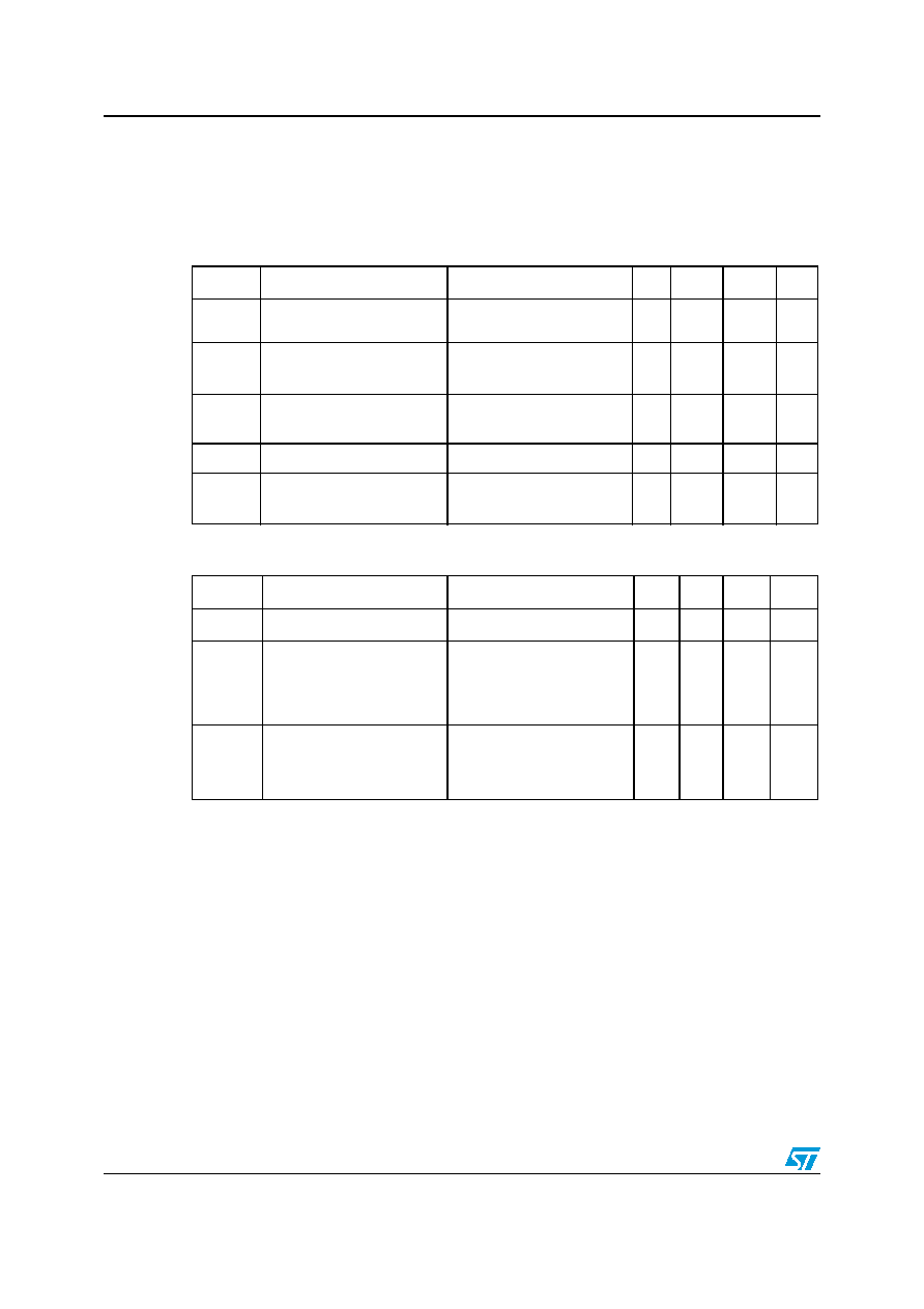
Table 2.
Thermal data
Symbol
Parameter
Typ.
Max.
Unit
Rthj-amb
(1)
1.
When mounted on FR-4 board of 1inch
2
, 2 oz Cu and
10sec
Thermal resistance junction-amb
20
24
°C/W
Rthj-c
(2)
2.
Steady State
Thermal resistance junction-case (top drain)
1
1.2
°C/W
Rthj-c
(3)
3.
Measured at Source pin when the device is mounted on FR-4 board in steady state
Thermal resistance junction-case (source)
2.8
3.4
°C/W
Electrical characteristics
STK800
4/12
2 Electrical
characteristics
(T
CASE
=25°C unless otherwise specified)
Table 3.
On/off states
Symbol
Parameter
Test condictions
Min.
Typ.
Max.
Unit
V
(BR)DSS
Drain-source breakdown
voltage
I
D
= 250
µ
A, V
GS
= 0
30
V
I
DSS
Zero gate voltage drain
current (V
GS
= 0)
V
DS
= Max rating,
V
DS
= Max rating,Tc=125°C
1
10
µA
µA
I
GSS
Gate body leakage current
(V
DS
= 0)
V
GS
= ±16V
±
100
nA
V
GS(th)
Gate threshold voltage
V
DS
= V
GS
, I
D
= 250µA
1
2.5
V
R
DS(on)
Static drain-source on
resistance
V
GS
= 10V, I
D
= 10A
V
GS
= 4.5V, I
D
= 10A
0.006
0.0075
0.0078
0.0098
Table 4.
Dynamic
Symbol
Parameter
Test condictions
Min.
Typ.
Max.
Unit
g
fs
(1)
1.
Pulsed: pulse duration = 300µs, duty cycle 1.5%
Forward transconductance
V
DS
=15V, I
D
= 10 A
44
S
C
iss
C
oss
C
rss
Input capacitance
Output capacitance
Reverse transfer
capacitance
V
DS
=25V, f=1 MHz, V
GS
=0
1380
450
75
pF
pF
pF
Q
g
Q
gs
Q
gd
Total gate charge
Gate-source charge
Gate-drain charge
V
DD
=15V, I
D
= 20A
V
GS
=4.5V
(see Figure 14)
13.4
3.4
4.5
nC
nC
nC

STK800
Electrical characteristics
5/12
Table 5.
Switching times
Symbol
Parameter
Test condictions
Min.
Typ.
Max.
Unit
t
d(on)
t
r
Turn-on delay time
Rise time
V
DD
= 15V, I
D
= 10A,
R
G
=4.7
,
V
GS
=4.5V
(see Figure 15)
15
50
ns
ns
t
d(off)
t
f
Turn-off delay time
Fall time
V
DD
=15V, I
D
= 10A,
R
G
=4.7
,
V
GS
=4.5V
(see Figure 15)
45
15
ns
ns
Table 6.
Source drain diode
Symbol
Parameter
Test condictions
Min.
Typ.
Max.
Unit
I
SD
I
SDM
(1)
1.
Pulse width limited by package
Source-drain current
Source-drain current
(pulsed)
20
80
A
A
V
SD
(2)
2.
Pulsed: pulse duration = 300µs, duty cycle 1.5%
Forward on Voltage
I
SD
= 20A, V
GS
=0
1.2
V
t
rr
Q
rr
I
RRM
Reverse recovery time
Reverse recovery charge
Reverse recovery current
I
SD
= 20A, di/dt = 100A/µs,
V
DD
=20V, Tj=150°C
(see Figure 15)
32
28.8
1.8
ns
nC
A
Document Outline