 | –≠–ª–µ–∫—Ç—Ä–æ–Ω–Ω—ã–π –∫–æ–º–ø–æ–Ω–µ–Ω—Ç: KBMF01SC6 | –°–∫–∞—á–∞—Ç—å:  PDF PDF  ZIP ZIP |
1/8
KBMFxxSC6
Æ
EMI FILTER AND LINE TERMINATION
FOR PS/2 MOUSE OR KEYBOARD PORTS
February 2002 - Ed : 1D
A.S.D.
TM
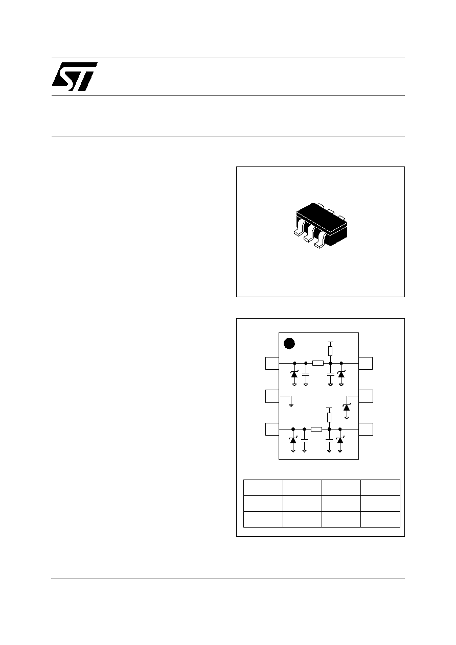
SOT23-6L
FUNCTIONAL DIAGRAM
TM: ASD and TRANSIL are trademarks of STMicroelectronics.
EMI Filter and line termination for mouse and key-
board ports on:
- Desktop computers
- Notebooks
- Workstations
- Servers
MAIN APPLICATION
s
Integrated low pass filters for Data and Clock
lines
s
Integrated ESD protection
s
Integrated pull-up resistors
s
Small package size
s
Breakdown voltage: V
BR
= 6V min
FEATURES
On the implementation of computer systems,
the radiated and conducted EMI should be kept
within the required levels as stated by the FCC
regulations. In addition to the requirements of
EMC compatibility, the computing devices are
required to tolerate ESD events and remain
operational without user intervention.
The KBMF implements a low pass filter to limit EMI
levels and provide ESD protection which exceeds
IEC 61000-4-2 level 4 standard. The device also
implements the pull up resistors needed to bias the
data and clock lines. The package is the
SOT23-6L which is ideal for situations where
board space is at a premium.
DESCRIPTION
s
EMI / RFI noise suppression
s
ESD protection exceeding IEC61000-4-2 level 4
s
High flexibility in the design of high density
boards
BENEFITS
Dat In
Clk In
Gnd
Dat Out
Clk Out
+Vcc
Rs
C
Rp
C
+Vcc
Rs
C
Rp
C
+Vcc
Rs
Rp
C
code 01
39
4.7k
120pF
Tolerance
±10%
±10%
±20%

KBMFxxSC6
2/8
IEC 61000-4-2 (R = 330
C = 150pF), level 4
±15 kV (air discharge)
±8 kV (contact discharge)
MIL STD 883C, Method 3015-6
Class 3 C = 100 pF R = 1500
3 positive strikes and 3 negative strikes (F = 1 Hz)
COMPLIES WITH THE FOLLOWING ESD
STANDARDS:
Symbol
Parameter
Value
Unit
V
PP
ESD discharge R = 330
C = 150pF contact discharge
ESD discharge - MIL STD 883 - Method 3015-6
±12
±25
kV
kV
T
j
Junction temperature
150
∞C
T
stg
Storage temperature range
- 55 to +150
∞C
T
L
Lead solder temperature (10 second duration)
260
∞C
T
op
Operating temperature Range
0 to 70
∞C
P
r
Power rating per resistor
100
mW
ABSOLUTE MAXIMUM RATINGS (T
amb
= 25∞C)
Symbol
Parameters
Test conditions
Min
Typ
Max
Unit
I
R
Diode leakage current
V
RM
= 5.0V
10
µ
A
V
BR
Diode breakdown voltage
I
R
= 1mA
6
V
V
F
Diode forward voltage drop
I
F
= 50mA
0.9
V
ELECTRICAL CHARACTERISTICS (T
amb
= 25∞C)
KBMFxxSC6
3/8
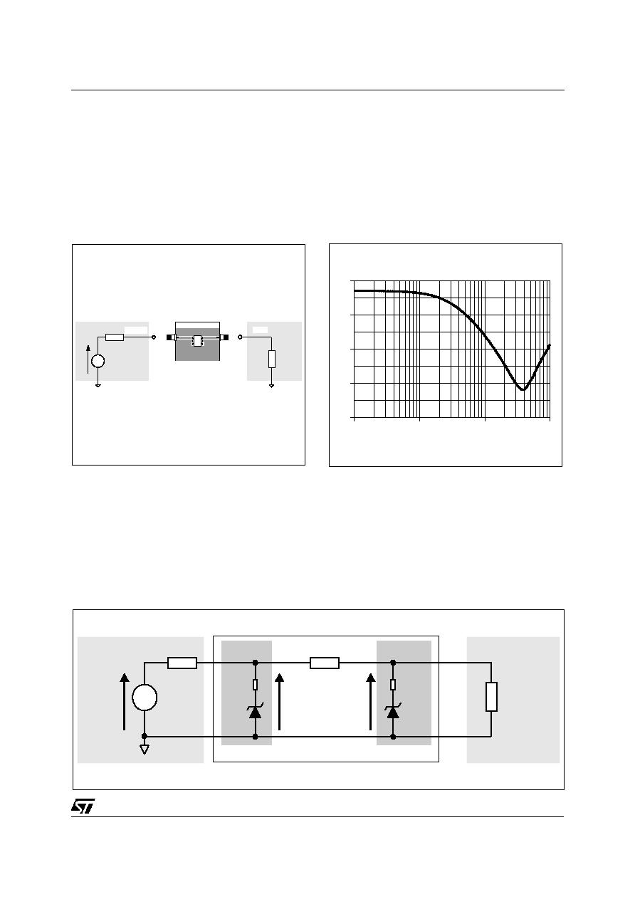
50
RF IN
Vg
50
TG OUT
TEST BOARD
KM1
Fig. A1: Measurements configuration
1
10
100
1000
-40
-30
-20
-10
0
F (MHz)
Insertion loss (dB)
Fig. A2: KBMFxxSC6 attenuation curve
TECHNICAL INFORMATION
The KBMFxxSC6 ensure a filtering protection against ElectroMagnetic and RadioFrequency Interferences
thanks to its low-pass filter structure. This filter is characterized by the following parameters :
- cut-off frequency
- Insertion loss
- high frequency rejection
EMI FILTERING
The KBMFxxSC6 is particularly optimized to perform ESD protection. ESD protection is based on the use
of device which clamps at :
Vouput
V
R I
BR
d
PP
=
+
.
This protection function is splitted in 2 stages. As shown in figure A3, the ESD strikes are clamped by the
first stage S1 and then its remaining overvoltage is applied to the second stage through the resistor R.
Such a configuration makes the output voltage very low at the Voutput level.
ESD PROTECTION
ESD Surge
Vinput
Voutput
Rload
Rg
Rs
S1
Rd
V
BR
V
BR
V
PP
Device
to be
protected
KBMFxxSC6
Rd
S2
Fig. A3: ESD clamping behavior

KBMFxxSC6
4/8
To have a good approximation of the remaining voltages at both Vinput and Voutput stages, we give the
typical dynamical resistance value Rd. By taking into account these following hypothesis : Rt>Rd, Rg>Rd
and Rload>Rd, it gives these formulas:
Vinput
R V
R V
R
g
BR
d
g
g
=
+
.
.
Voutput
R V
R Vinput
R
S
BR
d
t
=
+
.
.
The results of the calculation done for V
PP
=8kV, Rg=330
(IEC 61000-4-2 standard), Vbr=7V
(typ.) and Rd = 1ohm (typ.) give:
Vinput = 31.2 V
Voutput = 7.8 V
This confirms the very low remaining voltage across the device to be protected. It is also important to note
that in this approximation the parasitic inductance effect was not taken into account. This could be few
tenths of volts during few ns at the input side. This parasitic effect is not present at the output side due the
low current involved after the resistance R
S
.
The measurements done here after show very clearly (Fig. A5) the high efficiency of the ESD protection :
- no influence of the parasitic inductances on output stage
- Voutput clamping voltage very close to Vbr (positive strike) and -Vf (negative strike)
TEST BOARD
ESD
SURGE
16kV
Air
Discharge
Vin
Vout
KM1
Fig. A4: Measurement conditions

KBMFxxSC6
5/8
Fig. A5: Remaining voltage at both stages S1 (Vinput) and S2 (Voutput) during ESD surge.
Please note that the KBMFxxSC6 is not only acting for positive ESD surges but also for negative ones. For
these kind of disturbances it clamps close to ground voltage as shown in Fig. A5b.
The early ageing and destruction of IC's is often due to latch-up phenomena which is mainly induced by
dV/dt. Thanks to its structure, the KBMFxxSC6 provides a high immunity to latch-up phenomena by
smoothing very fast edges.
LATCH-UP PHENOMENA
a. Positive surge
b. Negative surge
CROSSTALK BEHAVIOR
Line 1
Line 2
V
G1
V
G2
R
G1
R
G2
DRIVERS
R
L1
R
L2
RECEIVERS
1
G1
12
G2
V +
V
2
G2
21
G1
V +
V
Fig. A6: Crosstalk phenomena
The crosstalk phenomena is due to the coupling between 2 lines. The coupling factor (
12
or
21
) increases
when the gap across lines decreases, this is the reason why we provide crosstalk measurements for
monolithic device to guarantee negligeable crosstalk between the lines. In the example above the ex-
pected signal on load R
L2
is
2
V
G2
, in fact the real voltage at this point has got an extra value
21
V
G1
. This
part of the V
G1
signal represents the effect of the crosstalk phenomenon of the line 1 on the line 2. This phe-
nomenon has to be taken into account when the drivers impose fast digital data or high frequency analog
signals in the disturbing line. The perturbed line will be more affected if it works with low voltage signal or
high load impedance (few k
).