 | –≠–ª–µ–∫—Ç—Ä–æ–Ω–Ω—ã–π –∫–æ–º–ø–æ–Ω–µ–Ω—Ç: L165 | –°–∫–∞—á–∞—Ç—å:  PDF PDF  ZIP ZIP |
L165
3A POWER OPERATIONAL AMPLIFIER
OUTPUT CURRENT UP TO 3A
LARGE COMMON-MODE AND DIFFERENTIAL
MODE RANGES
SOA PROTECTION
THERMAL PROTECTION
±
18V SUPPLY
DESCRIPTION
The L165 is a monolithic integrated circuit in
PentawattÆ package, intended for use as power
operational amplifier in a wide range of applica-
tions, including servo amplifiers and power sup-
plies. The high gain and high output power
capability provide superiore performance wherever
an operational amplifier/power booster combina-
tion is required.
October 1991
Pentawatt
Æ
ORDERING NUMBER : L165V
Symbol
Parameter
Value
Unit
V
s
Supply voltage
±
18
V
V
5
V
4
Upper power transistor V
CE
36
V
V
4
V
3
Lower power transistor V
CE
36
V
V
i
Input voltage
V
s
V
j
Differential input voltage
±
15
V
I
o
Peak output current (internally limited)
3.5
A
P
tot
Power dissipation at T
case
= 90
∞
C
20
W
T
stg
, T
j
Storage and junction temperature
-40 to 150
∞
C
ABSOLUTE MAXIMUM RATINGS
APPLICATION CIRCUITS
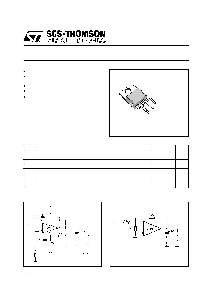
Figure 2. Unity gain configuration.
Figure 1. Gain > 10.
1/9

Symbol
Parameter
Value
Unit
R
th-j-case
Thermal resistance junction-case
max
3
∞
C/W
THERMAL DATA
2/9
PIN CONNECTION (top view)
SCHEMATIC DIAGRAM
L165

Symbol
Parameter
Test Conditions
Min.
Typ.
Max.
Unit
V
s
Supply Voltage
±
6
±
18
V
I
d
Quiescent Drain Current
V
s
=
±
18 V
40
60
mA
I
b
Input Bias Current
0.2
1
µ
A
V
os
Input Offset Voltage
±
2
±
10
mV
I
os
Input Offset Current
±
20
±
200
nA
SR
Slew-rate
G
v
= 10
8
V/
µ
s
G
v
= 1 (
∞
)
6
V
o
Output Voltage Swing
f = 1 kHz
I
p
= 0.3 A
I
p
= 3 A
27
24
V
pp
f = 10 kHz
I
p
= 0.3 A
I
p
= 3 A
27
23
V
PP
R
Input Resistance (pin 1)
f = 1 KHz
100
500
K
G
v
Voltage Gain (open loop)
80
dB
e
N
Input Noise Voltage
B = 10 to 10 000 Hz
2
µ
V
i
N
Input Noise Current
100
pA
CMR
Common-mode Rejection
R
g
10 K
G
v
= 30 dB
70
dB
SVR
Supply Voltage Rejection
R
g
= 22 K
V
ripple
= 0.5 V
rms
f
ripple
= 100 Hz
G
v
= 10
60
dB
dB
dB G
v
= 100
40
dB
Efficiency
f = 1 kHz
R
L
= 4
I
p
= 1.6 A; P
o
= 5W
70
%
I
p
= 3 A; P
o
= 18 W
60
%
T
sd
Thermal Shut-down Case
Temperature
P
tot
= 12 W
110
∞
C
P
tot
= 6 W
130
ELECTRICAL CHARACTERISTICS (V
S
=
±
15 V, T
j
= 25
∞
C unless otherwise specified)
3/9
L165
4/9
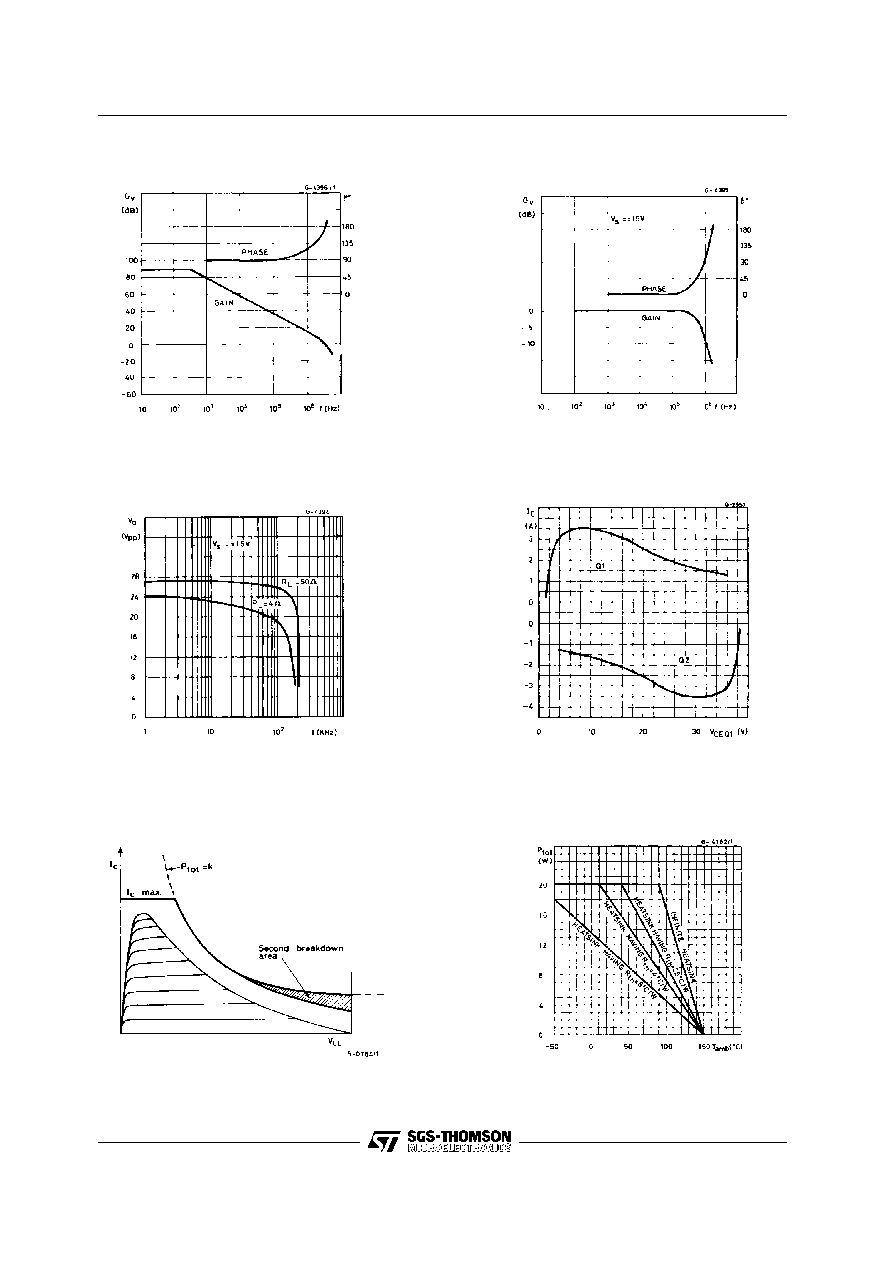
Figure 3. Open loop frequency response.
Figure 4. Closed loop frequency response
(circuit of figure 2).
F ig ure 5. L arge si gnal f re quency
response.
Figure 6. Maximum output current vs.
vo lt age [ V CE ] across each output
transistor.
Figure 7. Safe operating area and collector
characteristics of the protected power
transistor.
Figure 8. Maximum allowable power
dissipation vs. ambient temperature.
L165

Figure 9. Bidirectional DC motor control with TTL/CMOS/
µ
P compatible inputs.
Must be V
S2
V
S1
E1, E2 = logic inputs
V
S1
= logic supply voltage
Figure 10. Motor current control circuit with external power transistors (I
motor
> 3.5A).
D1 to D4 : V
F
1.2 @ I = 4A
t
rr
500 ns
Note : The inputvoltage level is compatible with L291 (5-BIT D/A converter).
The transfer function is :
I
M
V
i
=
R4
Rx R3
5/9
L165